Inside a Huge PCB Factory

Vložit
- čas přidán 11. 06. 2018
- You can watch this without ads on my streaming platform, Nebula! nebula.tv/videos/strange-part...
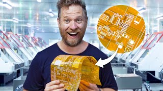
Today we're visiting JLCPCB (jlcpcb.com/e), one of the largest prototype PCB manufacturers in China. We're getting an exclusive factory tour of one of their newest printed circuit board factories in Huizhou, just outside of Shenzhen, to see the PCB manufacturing process step-by-step. Are you an electronics geek or a DIY enthusiast that loves soldering projects that's always wondered how to make that PCB? Today we're going to see how it's made!
Thanks to JLCPCB for sponsoring this video!
Share this video: • Inside a Huge PCB Factory
Subscribe to the channel here: goo.gl/qeurxc
Edited by auram - / aurxm
Gear for this video:
Main camera: amzn.to/2BfHqiW
Main lens: amzn.to/2BAysJQ
Other camera: amzn.to/2t1yKWi
Microphone: amzn.to/2kNCqHg
Wireless microphones: amzn.to/2t12jHJ
Audio Recorder: amzn.to/2sXTEWt
Facebook: / strangepartscom
Twitter: / strangepartscom
Instagram: / strangeparts_com
Music:
Shlow Motion Pt. 2 - oomiee (Licensed through Epidemic Sound)
Young Bones by Jake Maynard - Calaveras (Licensed through Art List)
Water - Seamus Mcnamara (Licensed through Epidemic Sound) - Věda a technologie


You can watch this without ads on my streaming platform, Nebula! nebula.tv/videos/strange-parts-inside-a-huge-pcb-factory-in-china
This video is because of you! I went through all of the comments from the previous factory videos, and seeing inside a PCB factory was one of your top requests. So keep the suggestions coming! I'll try and make as many of them happen as I can.
Strange Parts u allwayz great 👏👏👏 each like is deserved for U #congrats
I love your factory videos!
Yhea
Your channel is the only one I can watch every video from start to end no matter how long it is. The longer the better! Awesome job, love this kind of content!
Strange Parts go to OnePlus and look at there factory to make the OnePlus 6
I think Lily really enjoyed the tour of the factory, she learned a lot from the tour guide.
Yeah
James Kim exactly what I thought
@@fian3851 xD
She just could not explain all that in english. But you're right, it looks very strange.
@@0scur0_ It's pretty obvious her English isn't too eloquent mate. _Many_ Chinese people are afraid to speak English to a native (Mandarin's my SL). I imagine being on camera would be about 100 times more nerve wracking.
The background noise was rough and youtube's auto subs sucks, so I subtitled the video for you.
You're my hero, man. Thanks for doing that.
Thank you for doing this! We were debating baking in English subtitles, and decided against it. I always pay a professional service to add English subtitles, but they usually don't add them for a couple days. But helping me with subtitles is super awesome, particularly for languages other than English where I can't easily pay a service to do them for me. You guys are awesome!
you are the man bro!! thanks!
Nice dude. Your part of the reason I love CZcams.
many thanks for bro
I'm glad that Mr Liu was there to answer the difficult questions
yeah
yeah
I feel like strange parts said what the two people working there are supposed to say to the camera
lol he barely opened his mouth the whole process
yeah
Low cost aside, the quality of such a complex process is amazing, thanks to JLCPCB for allowing this tour.
bot 🤖
😂
50% enthusiasm
50% "yeah"
Connor O’brien “yeah”
100% YEAH
Yeah
Batt yeahh.
@Sultan Ali Khan Ohh yeah com Ohh yeah come on babe .
How it’s Made with actual personality! Awesome, keep up the great work Scotty.
Needs more horrible puns tho...
So well put. Watching Strange Parts become more and more professional has been very awesome to witness. I think we all knew what was coming from the first video though.
Exactly what I was thinking. Strange Parts meets "How it's made". Part Vlog part documentary. Excellent work.
Yeah, just add the annoying voice. Sorry how it's made guy
Scotty makes extra effort to make sure every step in the PCB manufacturing well is explained really well. This is something not easy to find in any book or by googling. I was just starting to learn PCB design and I was lost in so much terminology but this priceless video has cleared my confusion
he's talking more than the host
@@lancelydeEnglish language is not very easy
he's doing all the talking better said :)
@@lancelyde
Just ordered 20 boards from these guys. It amazes me the great value that you get considering the complex manufacturing process they go through.
Do they ship 20 boards also?
@@user-bq3sc8iw1i Yes, they accept orders for small quantities of pcbs, I saw a lot of people on the Chinese video platform bilibili share that they can get 5 pieces of pcbs for free, of course you need to design the circuit yourself
@@jsshao9523 do they ship to Nepal?
Who are you,sir?
Honestly JLCPCB have nailed it, their business is perfect. I got 10 small boards for 2 dollars plus shipping. Plus the quality control shown in this video. No one can compete with that. They deserve all the customers they get. I wish other chinese manufactures would understand the importance of quality control.
Ironic that Voltlog was talking about how a great deal JLCPCB is and then I watched this...how can ya compete against this! (I almost wished I could design a PCB to have them make for me) :)
They've really been advertising lately. I heard from a friend that the 2 dollar PCB thing is only temporary, but I hope it's not (if somebody else knows) so I can get some boards printed soon.
Spirit 6ish dollars for shipping is still low as balls compared to the competition
Shipping was a bit slow to the UK, but the PCBs were top quality when I got them. Will definitely be using them again!
It's almost unbelievable how much it takes to do all this, how well it's done and all the people and machines involved. I was super impressed by them. If I was making a product, I'd definitely check them out. It was all super interesting.
I freaking love this. The content, your sheer enthusiasm, everything in this channel is something I never knew I wanted or needed in my life. Thank you man. I’d love to see the process of making a GPU in a factory
Victor Panunzio doubt amd or Nvidia would be super happy with Scotty being able to expose tons of secret projects. Hes a sound guy but they won't risk anything
Hardrive33 yeah true, but maybe just a snippet of the assembly process would be cool to see
Well AMD and NVIDIA will just be for the silicon and own-brand components, and they've let others in before. companies like ASUS, EVGA, MSI, ZOTAC just buy the chips and put the silicon and memory onto boards they design with their own power delivery and aesthetic choices.
AMD and NVIDIA are both fabless. They only build designs. I believe TSMC does most of the fab work for both companies.
Amlogic or Rockchip
Don't take it wrong, Scotty actually the guide there. Lilly seems enjoy the trip in the factory. XD
Great content as always Scott! I work in PCB manufacturing as a cad operator, PCB manufacturing is a complicated processes. Your explanation of each manufacturing procedure was simple, very detailed, and by far the most consistent and accurate. Please keep up the great content!
After watching this video, I learned a lot. I could n’t sleep all night.
and my ears still seem to hear Lily ’s voice:
"yeah"
Yeah
Yeah
Yeah, her reaction is like the first time I saw a foreigner when I was very young😅
As someone who maintains automated machinery this tour of the JLCPCB factory was totally awesome. Thank you Scotty, I cannot wait till things level out and you can get back to bringing us to more super cool factory tours. Hang in there my friend, we are all in this together.
As someone who doesn’t care, thanks for letting us know.
How many times does Lilly said "Yeah":
1. 0:57
2. 1:05
3. 1:09
4. 1:15
5. 1:35
6. 1:39
7. 1:45
8. 1:49
9. 1:53
10. 2:06
11. 2:13
12. 2:15
13. 2:17 x2 in same sec => 14
15. 2:20
16. 2:21
17. 2:28
18. 2:41
19. 2:44
20. 2:58
21. 3:00
22. 3:03
23. 3:09
24. 3:14
25. 3:21
26. 3:28 x2 in same sec => 27
28. 3:37
29. 3:42
30. 3:49
31. 4:14 x2 in same sec => 32
33. 4:20
34. 4:25
35. 4:28
36. 4:46
37. 5:04
38. 5:06
39. 5:20
40. 5:28
41. 5:39
42. 5:45
43. 5:53
44. 6:09
45. 6:20
46. 6:37
47. 6:42
48. 6:48
49. 7:02
50. 7:08
51. 7:20
52. 7:36
53. 7:40 x2 in same sec => 54
55. 7:51
56. 7:53
😂
Why are people complaining about him repeating everything she said? He's doing it on purpose so we can fully comprehend and actually hear what it is she's saying. Without his commentary I would have missed a lot of what she was saying and had to replay and turn things up just so the details weren't missed.
His repetition is also for clarification, so that something hasn't been lost in translation. He repeats back to her what he understood about what she said, so that something wasn't misunderstood.
Yep, that was my intention. Ultimately, what matters though is how it makes people FEEL. And I'm definitely hearing loud and clear that the interaction with Lily felt off in this one, and that I was being disrespectful to her, or conversely that she didn't know what she was talking about. And I feel really terrible about that.
I think this was largely due to my nervousness and inexperience as a host as desire to make sure we covered everything I thought was important, but also was partly due to the way we edited it. As soon as I saw the first cut, I knew it was going to make me look like a dick. But we couldn't reshoot it, and we were struggling to keep the overall video to a reasonable length, and so at the time we felt like we were often forced to use my rephrasing instead of her original, longer explanations.
What I didn't realize at the time was how strongly people were going to react to this. I wish I'd acknowledged that it felt off at the beginning of the video, and definitely have a lot of thoughts on how I can be a better host and interviewer in the future.
I'm still proud of this video, and have high hopes and expectations we can make some more great factory videos in the future that feel less disrespectful and awkward.
Do remember that the vast majority of people who were pleased with this video will not say anything and that it is the nay sayers who will feel obliged to comment. People love to complain. Often just for the sake of complaining.
You've got almost 800,000 views on this with 31k thumbs up and only 702 thumbs down. Those are pretty good statistics. You can bet the people who are complaining are going to have hit that dislike button super fast. And also that the majority of people who actually liked it won't have bothered to click anything, so the numbers are even more in your favour.
The point is there are always people who complain, you cannot please everyone. You did what you thought was necessary to make the footage you had clear and understandable - you were right to make that decision. If a few people don't like the presentation then so be it, but you can be sure that if you had done something differently here there would be people complaining about that too.
Thanks for the support. It's very easy to focus on the negative comments, and ignore the positive ones. So I genuinely appreciate the reminder. At the same time, definitely viewing this as a learning opportunity to be a better host, interviewer, and storyteller.
I work in PCB assembly in America, and I think this video is great and informative! Thank you!
Hey man this video is really great, but perhaps you could use a translator/fixer in the future so that it makes the interviewee as well as the interviewer more comfortable in the situation? Coming from experience, just having someone in the dynamic that speaks the same language helps to keep the dialog flowing. Thanks! max
Really enjoyed this Scotty. You've produced content on par with the quality I would normally only be able to watch on a BBC television documentary. Thank you for your hard work and I look forward to seeing where you go next.
exactly, very professional content.
If the BBC had made this is would have needed two new managers to be employed a committee and a £200,000 spend.
I had some boards manufactured by JLCPCB recently. Love their work - and they are ACTUALLY as fast as this video makes out. Its seriously super impressive.
Huge thanks for this video, both for the maker of this video and for the guys at JLCPCB for the amazing factory insight.
Really appreciated it 👏😃
Please go to a battery cell factory - Lipo or Li-ion
Xavier Ancarno that would be awesome
That's a good idea, that would be very interesting to see.
I would love to see that as well! :)
hell yea !
Yes!! I would love to know how lithium ion batteries are made. Especially since they are almost everything these days.
You are one of the reasons why I've made up my mind to apply for a university in China and study in Engineering. Thanks for the inspiration and insight, really.
Hmm from your name i would assume you would go and study Mycology. :)
sorry bad pun
Stupchek lmao
Stupchek lloooollll
Stupchek
lol the pun
I am afraid you got it all wrong man. China did not invent those machines and the engineering behind it. They were introduced and taught by Taiwanese, Japanese and western countries back in the 1990's. China simply copied and used the engineering to build bigger factories to mass produce products.
This was one of the most interesting and understandable videos on PCB production. Great job and I hope to watch all your videos as time permits.
Me: OMG Lily, you are really cute!
Lyli: Yeah
Yeah
I'd love to see a silicon foundry making simple parts. Not like CPUs/GPUs/Memory, but ASIC/"glop tops"/mask ROMs, things like that. Things that are basically one-offs rather than mass produced
Given the engineering that goes into the equipment and the process I can understand why ASICs cost so much, I mean if 2/2mil spacing and microvias costs an extra 30~50% on a PCB, then imagining what a 80nm process must cost is not even funny.
Maybe a Texas Instruments stuff producer would be interesting
The PTH (plating through-hole) process is very complicated but I'll try my best to describe what's happening.
----- DESMEAR -----{1,2}
It all begins with the desmear which usually consists of 3 different process baths and is necessary for two reasons. First of all, one has to remove the so-called smear (all the stuff that forms due to high temperatures during the (laser)drilling process), debris and dirt. The other reason for the desmear is to roughen the surface so that the deposited copper adheres better. The first bath in the desmear process is called sweller and contains chemicals that permeate into the cavities of the base material (the glass fiber epoxy resin composite) thereby letting the base material swell up, hence the name. The second bath is often referred to as the actual desmear and contains a concentrated solution of alkali permanganate and hydroxide. Under these conditions organic materials, such as the smear, decompose and glass is etched back. The third bath contains reducing agents that help to get rid of permanganate and manganese dioxide residues.
----- PRE-TREATMENT -----
The next process step is usually referred to as the pre-treatment. It is composed of up to 5 process baths. Please keep in mind that i'm only explaining the most common type of process which is an ionogenic palladium activation process (other activation processes such as colloidal palladium (as explained in a recent video by applied science) and direct plating processes that work without any but one pre-treating bath also exist and are used in the industry).
(1) Conditioner
The conditioner contains chemicals that help the activator to bind to the surface of the base material and copper.
(2) Etch Cleaner
The Etch Cleaner contains agents that remove oxide layers on any superficial copper.
(3) Pre-Dip
This is a bath containing chemicals that protect the activator from drag-in and helping the activator to get even into the smallest VIAs.
(4) (Ionogenic Palladium) Activator
The activator basically contains cationic palladium compounds that can bind to the base material. Check out the palladium price in order to understand why this process is so expensive.
(5) Reducer{3}
The reducer contains reducing agents, that reduce the cationic palladium [Pd(2+)] to elemental palladium Pd(0). This is important in the subsequent step, as the Pd(0) acts as a catalyst.
----- COPPER PLATING -----{4}
Following the pre-treatment comes the electroless copper bath (ECB). This bath is used to deposit a thin layer of copper (usually around 1 µm give or take) that makes the whole PCB conductive so that it can then be plated in a conventional galvanic copper bath. Besides copper the ECB contains a reducing agent, alkali hydroxides and complexing/chelating agents as well as often stabilizers. The Pd(0) on the surface of the PCB catalyzes a chemical reaction in which the reducing agent is able to reducer the cationic copper Cu(2+) to elemental copper Cu(0). Since this reaction is autocatalytic it keeps on going once the palladium is covered in copper. However, the copper deposition using an ECB is very slow, expensive and doesn't give a nice surface finish. Therefore, the PCB is only treated for a short period of time and a galvanic copper bath is used in order to plate the desired thickness (commonly around 25 µm). The galvanic copper bath contains different chemicals (called leveler, brightener and suppressor) that help with via filling, surface finish, etc. .
Keep in mind that the overall process leads to an entirely copper covered PCB so structuring is once more necessary. Afterwards the superficial copper tracks, pads and so on are covered with tin in an immersion tin process or with gold in a nickel/gold process. This is necessary because soldering to the bare copper is very difficult since copper oxide layers will trouble the solder adhesion.
----- References -----
{1} J. Kirmann, X. Roizard, J. Pagetti, et al., J. Adhes. Sci. Technol., 1998, 12 (4), 383-397 (doi: 10.1163/156856198X00100).
{2} K. L. Mittal., J. Vac. Sci. Technol., 1976, 13 (1), 19-25 (doi: 10.1116/1.568850).
{3} O. A. Sadik, H. Xu, A. Sargent., J. Electroanal. Chem., 2005, 583 (2), 167-175 (doi: 10.1016/j.jelechem.2005.05.013).
{4} M. Paunovic., Mod. Electroplat., 2010, 1, 433-446 (doi: 10.1002/9780470602638).
If you don't have access to these publications, try using sci-hub... looks dodgy, is used by many scientists=)
+Nori-Atnep Lynobrac:
Sound like there is some palladium on PCB boards. But how many mg and is it worth recovering?
Shut up
Nori-Atnep Lynobrac . Wow, thanks. I fully understand now!.
Awesome comment! Thank you for sharing!
Thanks for this comprehensive explanation. Next person who complains about useless youtube comments gets directed here!
2018: "I gotta put on this charcoal mask, this sucks"
2020: "Man I wish I had more of those masks!"
Yeah
first, I HAVE TO THANK ALL THE WORKERS IN THE FABRIK AND ALL THE PEOPLE THAT PROGECT EVERY THING... I just wish you all a lot of good health, and God bless you!!
What I find extremely impressive is not the factory itself but the fact that you can get boards manufactured by them with your own design for like 8$ delivered to your doorstep.
olbrzym11 - Not only affordable, but good quality too! this video shows very well how they manage to do that. I guess it's all a matter of scale and highly automated processes.
You can’t beat China for value. They can do anything and everything, fast and high quality. There are so many choices and so much competition.
I think it's great the that JLCPCB has reached out to the maker community. They have invested a lot of time and money supporting CZcams channels as well as providing a quality product at great prices.
they provide very good quality pcb at very good price. i once used uk local pcb prototype manufacture. normally, for four panel 210 pounds. it takes 2-3 weeks lead time. jlcpcb only cost about 30 pounds puls 16 pounds shipping fee. they are very fast. normally, i can get my board in one week. from china !!! they also provide online pcb software which is really better than some paid softare. very impressive!
Got my first 20 PCBs from them a few days ago. With some fancy options clicked and fast delivery to Europe it was $55, got them in a week (had to pay tax). Even for a noob SMD hand solderer they work fine.
Thanks to everybody involved, great video, great work man!
Let's not be unkind to Lily. He speaks quite quick and just as Chinese is one of the hardest languages for English-speakers to learn, it's probably the other way around as well. Also, she was probably nervous. I think she did very well!
Yes, she did fine, and he is a loud, brash yank, something very alien to the reserved Chinese.
This is legit better than 98% of TV documentaries. I hope you are being paid enough and receiving a great deal of satisfaction from this. You are getting seriously good at your job and your passion and it's great to see!
Lily is such a cute and fun rep.
Yah.
No!
The video just keep getting better! I had no idea you were doing a comprehensive tour of the whole board making process in the factory. Wow, I was entertained.
just sent of my first PCB to JLCPCB yesterday and was really interested to see how they do it... so cool to come back to this video and watch it as my own boards are going through the process!
Really enjoyed this! I have been ordering batches of boards from several Chinese PCB manufactures for the last twenty years. I know the staged pictures they like to send me in their digital "slick" sheets, but it's nice to see inside of an actual factory.
yeah
I think it’s more amazing to see how people actually design these boards! It’s so detailed and amazing sometimes I just look at my phone and just become in awe of what humans can do.
Delywx Yap If you're interested, check out my company channel under rpcelectronics. I have tutorial videos on creating PCB layouts.
I've got a recurrent nightmare where I fall through a time-portal to the past.
Pull my phone out of my pocket and after dodging being burnt at the stake, decide to share the millennia of knowledge that's been subsequently accumulated...
...and then realize I literally haven't got a clue.
Then the phone battery goes flat and interest is lost in me.
I spend the rest of my remaining life being the "mad guy who can just about guide an oxen to plough a field"
NO Modern Tech is possible without all Inventions that had been invented in the Past. It's a step by step process. Just think about it like the Chicken and Egg Problem. How can PCBs made without machines that use PCBs?
For your Nightmare...learn common Stuff of Chemistry and Engineering from 18/19th Century. That's more then enough, even to Charge your Phone.
This was an incredible video! Its amazing how much access they let you have to be able to show each step. I had a lot of fun learning just how many steps there actually are in making a board , and to think they can get it done in roughly 24 hours. Thats almost TO efficient lol.
yeah, it looks difficult
Don't you know? It's because of the kitchen nightmares!
The reason they hide the kitchens is because most US kitchens won't pass the strict inspection at any moment
I made a board using the same methods but at home.
You can see the process on my blog: howtoengineering.com/2014/10/make-a-circuit-board/
It was a fun process and much simpler then the methods on this video.
I am sure you could never do that kinda tour in most country at all as there would for sure be Intellectual property/copyright issues.
the volume and speed of board production here is insane considering how customizable everything looks! the entire manufacturing process looks really well thought out. did i miss info on how long that plant has been operating? would be interesting to see how they started before scaling up to this.
Really great video. Just did my second order with JLCPCB and I am really impressed with them. They definitely have the whole process dialled in.
I get my hobby boards manufactured by this company. 4-6 days from submitting my files to delivery at my front door. And at US$0.20 cents per board. Fantastic service.
maybe you guys can help im trying to get a 26pin ffc .5mm pitch to a 2mm pitch 26 dip. What will be the easiest way to get this board made up.
This is good to know
Twenty cents per WHAT?
Twenty cents per board. Yes they charge $20.00 for shipping but that gets to my door in New Zealand in 3 days. There is an option of "slow boat from China" for about $10.00. The cheapest option in NZ was $24.95 per board ($249.50 for 10 boards) plus $10.00 shipping
hoppynaki hi, do you have any contact details please?
JLCPCB. I have ordered a lot of boards from them. 2 layer, 4 layer, 6 layer. Some boards were production boards that I ordered thousands of. Very high quality boards very cheap and very fast. Recommend them.
I started in IT back in the late 70's. My mind is blown by the miniaturization and compression that has been made. Also the speeds ... started with a Pet Commodore with a 1 Mhz CPU, 300 baud acoustic coupler, and cassette tape storage... Yes Mhz... things have come a long way.
For me I started in the 80s, where a floating point unit would be an external unit. 40MHz 386DX, the increase is nothing short of incredible. I wonder what computers in 20 years will be like...
Thanks for the factory tour.
I am a hobbyst and purchase from JLCPCB at least once a month.
I must say that quality is top notch and affordable therefore Q/P ratio is huge.
And fully customable in size and color and whatnot.
After I discevered I can design my own PCBs and let them produce them... Extremely happy!
Dude, that is a GREAT format for you!
Thanks! We worked super hard to develop the factory tour format in this video - I'm glad it shows:)
It really does! I was loving the plain tours, but this video is a lot more involved in the manufacturing process. I would go for injection plastic and cable looming next! :)
Yes Scotty, this is definitely the right direction for you and the channel. Looking forward to more content like this.
Is she giving you a tour or are you giving her a tour? Haha :D fascinating factory, great video, documentary level!
I imagine that the factory representative explains each step to the visitor, and then he repeats a more succinct version to camera, and that's the one we see.
he can be annoying but awesome video
Lol, come on guys, give her a break, she clearly doesn't speak very good English (I know first hand that it's very difficult to practice * speaking * a foreign language in your own country :P) plus Chinese people are usually not as much outspoken as other people.
Travelin: Be nice if she was given a chance to explain not bulldozed all the time by an egotist.
hes too hyped in this video apparently
I was chief engineer at a PCB shop in California. You missed one step in between drilling and plating. Multilayer boards need to be either plasma etched or chemical etched (opposed to alkaline etch) so the vias and plated hole achieve a three point contact with inner layers. Coming to plating question. Essentially copper in the plating solution is in divalent state (+2 state). The copper needs to be reduced to metallic state (0). Theway tis is done is reduction of valence states. The first application of copper is via electroless copper. This plating bath is called electroless because it uses chemicals to reduce copper to (0) valence state.
The copper build plating bath uses electric current to reduce copper to (0) valence state.
Hope this make the plating process clear to you.
I am retired now and was connected to PCB industry for 40+ years.
Thanks for the visit, very interesting to see the steps in sequence with some explanations. And I still cannot fully comprehend how the resulting PCBs can be so cheap despite the complexity of the process and the significant machine time needed (notably drilling and testing).
The first copper plating line you saw was called Electroless Copper Deposition, it is a process that is used prior to electrolytic copper plating, it deposits micro inches of a fragile copper in the holes to make them electrically conductive for electro copper plating, without that step copper will not be plated on to any surface that is not electrically conductive (pre preg layers in the holes)
micro inches !!!
Sundhararajan Ganesan
µ inches indeed!
Awesome - this more or less matches my understanding, but I didn't feel confident enough to try and explain it on camera. Thanks for clarifying!
Strange Parts You did a good job at it I just happened to type this reply when you were asking for a chemist to explain it. Thanks for the awesome video.
In the Electroless Copper Deposition process, palladium is first 'deposited' (not electroplated) on the walls of the vias and also the 'desmeared' surfaces of each 'inner layer' of copper to be connected. Copper will then 'stick' to the palladium to make the 'micro-inch' thick conductive layer, ready for subsequent copper-plating. Without the palladium, copper will not evenly deposit on the fibre glass surface.
You're probably the most enthusiastic man I've ever seen visiting a circuit board manufacturer. Great video!
Man, those PCBs are so exciting!
Absolutely brilliant! I am amazed at how efficiently and accurately they can do this. So cool!
Great video! I've had PCB and Flex made in US but never seen a full factory video like this one. Well done.
Mannnn. Not that your editing was ever bad (it has always been really good) but this is just awesome. I love all the little effects that you put in. it really makes it very interesting to watch. Nice Job
Yep - Kevin, my editor, really hit it out of the park on this one!
did he do it with the PC linus built :p
The mexican guy. Just like me :'(
Tell Kevin its awesome :)
They actually giveaway the Linus built computer
11:43 Strange parts: Now we need to drill the holes.
Lily: Whaaat??
Strange Parts: All the holes.
Lily: yeah
14:30 Strange parts: The first step gave us enough copper to do this, and then this will.... GROW THE THICKNESS OF THE COPPER IN THOSE HOLES.
@@thomaself7194 😂
She thought he was talking about her ;)
We will bang okay?
Lily : My body is Ready...
Lilly*
Amazing process, thanks for showing how it's done ...
AMAZING i made my first pcb 10 days ago and they arrived already, boards made and fully working, such a great company to deal with.
maybe visit a TV factory! Or something super unusual
I wonder if he could also go to Germany to maybe visit a factory where robots make/assemble machines that make robots. :p
A display manufacturer would be awesome. Maybe TCL is a good option? They are based in China and design/manufacture all their displays.
TCL are around the 3rd largest manufacturer now too
Felix Kütt robots making robots, awesome :D
Too bad no one (at least that I can think of) makes plasma tvs anymore. Not even sure if that would make a good video, but I still think they're cool.
Incredible video, I'm Chinese, I also find Lily's English is limited, so I'm so thankful Strange Parts translated them into English-friendly language.
THIS, is like what I'm seeing in Discovery Channel!!
其实我很想知道这个中文字幕是怎么来的……
@@user-io9xg4fw4l 自动翻译的吧
I don't know what the last two replies said, but I feel like you just got roasted
@@alexiscarrillo7305 there are some mistakes is Chinese subtitles……
@@beitewu2502 Nice one, that's exactly what I was thinking.
I just did my first PCB ever. I am an electrical engineer but in most Aerospace and Defense companies, we don't do our our own PCBs, we have a group that does that for us. So I needed a PCB for a home project and knowing the basics from working with PCB designers over the years, I designed my first. I chose JLCPCB and they were great. They rejected my Gerber files 4 times until I found the "secret sauce" to set up all the proper options for my Gerber files. They were very professional and insured I gave them a sound design before they went into fabrication. You can watch the status of your design at each step in the process. It was only about $8 US for 25 two layer PCBs that were about 1.5 X 0.75 inches. Once I clicked the 'approve' button, my PCBs were finished in about 36 hours.
I was using PCBway for years til I found these guys , these guys are the best . I`ve been using them now for a long long time and they never let me down the lead time is amazing , and every board comes to me just as I wanted it . Way cheaper than PCBway too ! Thanks guys you really are the best!
Now we know why China is an electronics manufacturing hub. Their factory lines are so efficient!
I am from ShenZhen.. it is one of the small factories, there r plenty of them, U guys can come to Shenzhen and take a look, experience it, hope people around worlds would stop racism on hard-working Chinese people.
Hi,Man
I love the way he go to ur work place, explain all ur work process, so all u can do it to say YES.
Wow, this process is really amazing!
I've been designing and dealing with the manufacture PCB's for over 33 years and know the process, but this video was great!
Could you please tell me what is Gerber file
You can easily google it fam!
Absolutely amazing process. I was spellbound by the complexity of the process. I always wondered how much effort went into making boards as efficiently as possible
Thank you so much for sharing this video, it was so insightful.
Congratulations to all the people who work with this company. I find this stunning to watch and I must admit that though I have had many affiliations with industries and universities over the last 80 years , I have never seen such brilliant work. Behind those machines there are many people who know much more than the people who simply are proud to own what they can buy. Modern industries have became an engineering art that only a few can comprehend. Congratulations once again and thank you once again, I feel rather excited by what I have just seen. This is sublime ----of very great excellence and beauty:
это точно. Какие инженерные умы !. Это потрясающе.
He comes off as genuinely a sincere and nice CZcamsr of China. He seems to respect Chinese and her culture the way they are. Unlike other foreigners CZcamsrs who always to find faults about China.
Leslie Cheung SerpentZA?
Theo Valentino lol
Well, there are many sides of China...this is only the glory part
oppressive regime , human rights abuses look into the channel china uncensored to learn more
Well. it looks like you are giving her the factory tour.
You have amazing knowledge.
She was giving the factory tour, but I ended up re-explaining a bunch of things for clarity. In the end I think we can say it was a team effort:)
Strange Parts yeah, the editing seems like you were teaching her lol, great video !
imho the video makes scotty seem a bit condescending but I'm sure he wasn't.
omsonic no offense to chinese people but english is not their forte Im not surprised at all they had to cut out most of their explanations. Its already a long video how it is
not offense to American people , but chinese is not their forte........
Awesome tource, great video. I spent every second viewing it over and over
*Thank you for upload this and remember YEAH!*
This is so fricking interesting! Amazed that the factory owner is ready to provide this detailed insight to "just a youtuber". Really a sign how far independent quality content has come.
I'm so pleased you made this video. After creating my own PCBs for years I recently ordered my first set of 5 PCB's from JLC. I've always been worried that my designs would come out wrong but I needed some PCBs with pads and traces too small for me to make. I was very impressed with their service. Because it was my first order they didn't charge me shipping (which was more expensive than the PCB's in my case) and the quality was excellent. Seeing this video just reinforces how professional an operation they have.
Crazy awesome factory! Next I need to find where you cover the process of soldering the electronics components! Love it!
22:41 “We have to make sure that the things that shouldn’t connect do connect and the things that shouldn’t connect don’t connect” 😂
Really like this documentary.
A suggestion if you do smth like this again. Maybe let the representative talk more. It seemed like you explained everything and she didnt even have to be there.
Kinda agree, maybe let them explain in Chinese and add subtitles after just like how documentation usually do.
Its a very technical process for her to explain in a secondary language, and from an editing point of view Scotty maybe didn't want to have to subtitle the whole tour. However for an automated PCB factory their setup is very common, just really big. So, I think Scotty did a lot of prior research and presented what he knew and she pointed out how their setup achieves these standard steps. He did an excellent job of explaining almost all the steps, in a lay person friendly way.
I agree.. Kinda makes her look stupid and ditsy. I'm sure she'd be able to explain everything in Chinese. I'd be fine with reading subtitles. Props to Scotty for thoroughly doing the research beforehand.
Yeah I agree. It looked like he was staff giving her a tour. She even looked a bit annoyed at times imo.
Yeah I was sort of feeling something similar, and it wasn't even that I wish she would have talked more, it just felt like he was explaining it to her, instead of explaining it to the audience. I understand language barrier stuff and I feel like he did that fine, but wording things differently and being more conversational with it would drastically change how it comes across, making it come off as him confirming what he's researched and asking questions, versus telling her what she already knows is happening. it wasn't really that bad though, there was still a decent amount of conversation and information from her.
Didn't show how they manage alignment - do they use x-ray to align with inner layers or just rely on the panel edge?
Would also be interesting to know how they keep track of designs through the process, making sure they get the right films etc.
Quote from one of answers: "They had some pretty cool machines for alignment, but we ended up cutting some of it out of the video because it was too long. They punch very accurate holes in the films, and punch matching holes in the PCBs. They had a couple different exposure machines - the one I showed I chose because you could actually see what was going on, but I think they used a different one with registration pins for the outer layers. It's still impressive to me that it all stays aligned though:)"
You basically just watched an advert, JLCPCB have been sponsoring lots of channels in recent months.
I'm sure it's money well spent, I was impressed at their facilities and will use them in future
Having already ordered from them in the past, they will add your order ID on the silkscreen (and most other layers too I guess)
1 cent has been deposited in your paypay accounts.
Impressive factory, really efficient-looking and clean. What's just as impressive and doesn't come out in the video is the organisational systems enabling an order goes from start to finish keeping all the layer, drill, print files together - perhaps sometimes different customers' orders on the same sheet to reduce waste - while not getting mixed up with other orders.
Great vídeo!!
I enjoyed the factory tou!!
Congratulations for the video, it's great! A few months ago I collaborated with them and they sponsored me a video. Seeing the finishing and quality of the PCBs I knew it was a great company, but what I could not imagine is how big and well prepared their facilities were.
Loved watching this video, opened my eyes to what actually goes on behind doors into making PCB"s.
Thanx for the good video. Keep doing what you do!!!
Shout out to Great Scott for single-handedly making sure I knew who JLCPCB was before I ever watched this video.
just realized they put this video on the homepage. Cool stuff man!
I'm confused, I thought the girl was giving him him a tour
Great video, Scotty! I knew a few things about how multi-layer PCB boards were created, but to see ALL the steps is SO cool. I have no idea how they do Inventory Control at that speed!
I learned a lot. Great video. Thank you.
Just received my 2nd order of custom boards from JLCPCB. I used to run a screen printing company and have produced my own diy PCBs so very familiar with the process. The quality from this company is unbelievable. I don't know how they do it for the price.
I am not sure how JLCPCB plates copper on their boards, but we've done this in our laboratory. Please research the process thoroughly if you attempt it, it uses toxic chemicals, especially formaldehyde.
There are two steps: first electroless plating, then electroplating afterwards. I can explain how we electroless plate our 3-D printed parts. First they must be cleaned thoroughly, which for example can be done by using sodium hydroxide. Then the surface must be made hydrophilic by oxidation. We use hydrogen peroxide or sodium percarbonate for this, others use ammonium persulfate. Then we have to put a catalytic layer so that copper deposits on the surface. We use colloidal silver as our catalyst, which is deposited by alternately dipping in silver nitrate and tin (II) chloride. Then electroless plating is performed, with a mixture of EDTA as a chelator, triethanolamine as chelator and buffer, sodium hydroxide, copper sulfate, and formaldehyde as the reducing agent with the solution maintained at pH of 11 and at 50-60 C. Then the part is electroplated, which uses dissolved copper in an acidic solution, with copper sulfate, acetic acid, citric acid, and a few other chemicals that act to make the electroless deposition smoother, more even, and shinier. Then it is dipped in a protective solution like benzotriazole to prevent corrosion on the surface.
The process we used is for an academic laboratory, so its likely JLCPCB's is more suited for mass production and not like the one I've described.
Ordering boards off these guys is so cheap you might as well have them do it :)
Formaldehyde is good, it gets pumped into you vains after you die, keeps the worms away.
SittingMoose Shaman what is your point? You are using electric are not you? If you didn't know that kills you and the planet too.
The first plating was a cyanide strike. The second was a common acid bath. Both are variations of electroplating.
I really enjoyed this vid! It feels like you're really inside the factory for a tour. Thanks Scotty for making this vid!😊Hoping for a much more factory adventures!
Loved that intro shot where you stepped forward and the camera "dollied" backward until your interviewees came into frame. Really slick.
amazing. just placed my first orders with them, had no idea it was this complex and took this many people and factory space.
These guys are mind blowing. I sent in my pcbs design from Australia and i had the board in my hand 7 days later!!!!!
The speed of this operation has unlocked a new superpower for me in board production, soon cheap and ultra fast
You gave her a great tour...!
Dor Amram 😂😂
At 6:35, Its not Blue light, the photoresist coating or film is sensitive to light of lower wavelength specially UV. Therefore, in a CLEAN ROOM, where you were, always have Yellow light which theoretically cannot react with the photoresist. The whole process is called Photolithography.
they are so fast i submitted my order today and got it yesterday.
but it is insane, made my own board had it within a week saved so much time and my project less wires to worry about making. made it more reliable and compact. for 27 canadian
I have almost no interest in electronics and how they work, but his enthusiasm makes me interested! Seriously love this guy's content!
you will be interested when you know he is a multi millionaire
Is that your Google Account?
+Google Account commentator**
Thank you so much for this,this is amazing it definitely changes the "made in china" mentality. Love these videos keep them coming :D
Type your Name There are many high tech things in China that are not shown. Its confidential.
There are certainly also many non-glamorous aspects that aren't shown either. E.g. leaded HASL, occupational safety and especially lax environmental regulations.
yeah like the hot soldering mask room or the chemical byproducts of washing
In China, we can print it twice a month for free, and it's also free of charge. Thanks to Jialichuang, everyone can feel the power of science and technology.
Not a shameless plug, i don't even work for JLCPCB, but we do a lot of prototyping and JLCPCB became Nr.1 for our needs. They upgraded their capabilities a lot in the last few years. They can do filled and plugged vias up to 20 layers at a "unbeatable" price. Pretty reliable quality and production times also. Can't really say anything bad about them and i hope the people who are working there are treated well.