Can you please make a detailed video on how semiconductors are practically manufactured by doping silicon crystals with Boron, Phosphorus and other substances? Because that's the basics behind the manufacturing of all modern electronics. No one on CZcams shows how silicon crystals are practically converted to N-type or P-type semiconductors and other stuff like that. I enjoy watching your channel and learning since 4-5 years and I must say, you guys are the best!
they use this exact same process, just at a nano scale. They use basically atomized atomic sources to "spray" atoms onto a substrate, and there are ways to mask. Most of the effort and work is building copper structures, the creating of transistors as you describe is only at the cores of the chips or storage arrays, in which case there are many ways to etch the little machines out of the surface
If one have access to a research nuclear reactor, the thermal neutrons it produces can be used to irradiate a Si ingot. Part of the Si consists of the isotope Si-30, which becomes Si-31, which in turn becomes P-31 by emitting an electron. This minute amount of phosphorus changes the silicon into n- type silicon.
This is NOT the “SemiConductor channel”…if you want Semiconductor specific info go to the Semiconductor channel! this is PCB (Printed Circuit Board) Channel !!!
The gold can perhaps be replaced into recycled aluminium in combination with recycled glass and plastic. Just a remark Thank you for this video, kind regards.
Can you make a video on glass used in making lenses? How are optics grade glass cut to make the appropriate light diffraction? How are incorrectly cut lenses cut to correct any imperfections?
It's a joke, they used random PCB 3d model in the video, not an actual airpod PCB, and when the video zooms in on it, you can see THT electrolytic capacitors with 63V rating on them, which in reality are bigger than the entire airpod itself, making it quite hilarious :)
Good video, albeit laminated PCB's aren't used for Ultra/HDI packaging applications like Apple Air Pods, which use thin-film ABF low temp build up process.
sir can we simulate and see the actual working condition of the circuit diagram when we use easy eda software , plz give us a link to down load it , teach us how to use it how to simulate a drawn circuit diagram
Please don't fool us again with these long form advertisements. This was such a step down from the quality of your normal videos. This explanation of the PCB production process was rushed and poorly explained. The video should have been twice as long and way more detailed. This was just a marketing gimmick for some shady PCB company that provided videos' to Lesics that didn't explain anything. I am staying far away from JLCPBP after this video.
Good work. Please higher the pace of releasing quality videos, hire teams of people, better production value would be very appriciated. Dont want to spend my whole life learning these concepts :D You are trully making difference in peoples lifes, Keep it up and hopefully beyond.
@@lewiskelly14 So what!. What's YOUR effort. A train trouble ad, who cares. Take a look at yourself! Make a Real effort! your 11 subscribers - justified.
Blessings in an abundance of the faith. I salute you. 😘🙏Grace and peace be unto you and to this place. God bless you. Thank you. Will you believe and receive Jesus Christ as your LORD and personal saviour??? I do. 😊
No, he meant magnetic field. Electricity and magnetism are very closely tied. The higher the current the stronger the field. If you put a compass near a cable with a current it will impact the comapss' needle. Magnetism can also produce the electricity, that's what call the electric induction. That is also why Sun can destroy all electric devices on Earth with strong magnetic winds.
@@bellzon4086 of course there is but electric field is more particles related. He said magnetic field because it is the one that is "making problems" in circuts, not the electric one.
@@bellzon4086 dielectric breakdown happens only when there is over current, while electromagnetic induction happens at any current with varying intensity of course
Ok. So here are few points you need to improve on: 1. 2:33 We don't use a 2 layer PCB just to reduce PCB size. A 2 layer PCB can have separate ground plane so that we don't have to route ground nets. Also it provide shortest return path and hence reducing EMI and improves signal integrity. Also, usually we don't add components on the 2nd layer of a 2 layer PCB! 2. 3:34 No explanation was provided for how adding ground plane reduces EMI. Pls refer Eric Bogatin and Robert Fernance videos for this! 3. 4:07 Those are stitching vias. Used to stitch two ground or power planes. 4. Instead of adding more related information, u want to extract gold from PCB! Why? Maybe you could have explained about the complete manufacturing cycle (Design, Prototyping, Manufacturing, PCB test gig, EMC compliance process, etc. I hope you will improve on this! Thank you!
What a narrow, selfish view…Did it ever occur to you that you are not they are not making these videos just for you? You the only one watching it…not everyone wants detailed info tangentially related stuff…
@@BoomBustProfits I see a partiality here! These guys explains the mechanical related stuff in depth but touches only the surface when it comes to the electronics part. Maybe I am selfish or maybe I just expect more from them! :)
Anyone here first to comment after watching the while video? Ya khali ye hi race jeetni hai sabji 😂 Also, disappointed to see such cookie cutter video from great channel who used to make quality content. This is just a promotional clip amalgamation of jcpclb or whatever and easyeda. This video should be on their channels.
Any promotional material should be marked as ads separately and not masked like this. I am sure there are other alternatives to these softwares. Promotion code in comments added sneakily without any mention in the video.


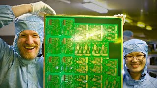


Hello everyone, we hope you enjoyed the PCB video. Now, get 1-8 layer PCBs at $2 and also get a $54 JLCPCB new user coupon from jlcpcb.com/RHS
No. Basically a sponsored video. Piss off.
where did you make the CG girl? which software?
Please convert to Indonesian leaguage
@@seabreeze4559 It's a Blender model
I have used this online it is very good
Can you please make a detailed video on how semiconductors are practically manufactured by doping silicon crystals with Boron, Phosphorus and other substances? Because that's the basics behind the manufacturing of all modern electronics. No one on CZcams shows how silicon crystals are practically converted to N-type or P-type semiconductors and other stuff like that. I enjoy watching your channel and learning since 4-5 years and I must say, you guys are the best!
they use this exact same process, just at a nano scale. They use basically atomized atomic sources to "spray" atoms onto a substrate, and there are ways to mask. Most of the effort and work is building copper structures, the creating of transistors as you describe is only at the cores of the chips or storage arrays, in which case there are many ways to etch the little machines out of the surface
If one have access to a research nuclear reactor, the thermal neutrons it produces can be used to irradiate a Si ingot. Part of the Si consists of the isotope Si-30, which becomes Si-31, which in turn becomes P-31 by emitting an electron. This minute amount of phosphorus changes the silicon into n- type silicon.
Try Branch education channel
Check out the youtube channel asianometry
This is NOT the “SemiConductor channel”…if you want Semiconductor specific info go to the Semiconductor channel! this is PCB (Printed Circuit Board) Channel !!!
How to get rich: Melt PCB's until you have enough gold.
😂
Or mine a compressed gold chunk out of Hoxxes. (ROCK AND STONE!)
Process of extracting gold will cost. 10× times than the cost of golf itself
Some waste management company does
God,that's poisoning
Mechanical engineering's capacity to the micro- nano level 🙏🙏🙏🙏
Basic electrical engineering
More an ad than an educational animation
0:54 love to see how she uses Windows in a Mac system.
Another great video btw!
Many people run Windows on Apple hardware with "Bootcamp"
Thanks for the PCB video, as always very informative
Great video. Can't wait for the reupload so I can watch it again!
This feels more like an ad.
Me all of a sudden thinking about my childhood's 8 bit video game cassette for gold extraction
It's probably worth more intact. Those things are really collectable!
@@3rdworldgarage450 commodore 64.. Amiga 500... these were the days
i used jlcpcb for all of my projects. they are cheap and reliable
This video deserves more likes!
this website is a really easy handle tool! i would like to comprehend things by doing. with this tool, i can understand PCB with much ease
Good knowledge, well done, thanks for sharing with us :)
The gold can perhaps be replaced into recycled aluminium in combination with recycled glass and plastic. Just a remark
Thank you for this video, kind regards.
Can you make a video on glass used in making lenses? How are optics grade glass cut to make the appropriate light diffraction? How are incorrectly cut lenses cut to correct any imperfections?
Wow so good explained 👏🏼👏🏼 thank u
Boy, those airpods are a true marvel of technology. 63v rated electrolytics in such a tiny package xD
where's the 63 volts?
It's a joke, they used random PCB 3d model in the video, not an actual airpod PCB, and when the video zooms in on it, you can see THT electrolytic capacitors with 63V rating on them, which in reality are bigger than the entire airpod itself, making it quite hilarious :)
Data and communication
Was absolutely fantastic.
59 rupees paid. Won't let this channel die
Thank you for the video!
Wow how much gold i could have get from all my broken laptop.
Great work THank you
Thanks for sharing 🤗
Excellent
Good video, albeit laminated PCB's aren't used for Ultra/HDI packaging applications like Apple Air Pods, which use thin-film ABF low temp build up process.
Verry nice👍👍
Great video
Thanks for the video
from Bangladesh 🇧🇩🇧🇩
how did you get the iMac to run windows though
Great explanations !
sir can we simulate and see the actual working condition of the circuit diagram when we use easy eda software , plz give us a link to down load it , teach us how to use it how to simulate a drawn circuit diagram
King video.
Japan has a shortage of raw materials so they have been perfecting the extraction of mentals from PCBs since the 1970s.
Great 👍
Can you please do one video on BMS BATTERY MANAGEMENT SYSTEM which is used in battery application Is electric vehicle
I literally read multiplayer PCB in the thumbnail lol.
So thats how pcb made
How do i get circuit diagram from existing PCB boards (just vice versa)
No one is first.
I'm always first
Thanks
Interesting!
You should upload a video of how a touch screen works
Nice video.
Please don't fool us again with these long form advertisements. This was such a step down from the quality of your normal videos. This explanation of the PCB production process was rushed and poorly explained. The video should have been twice as long and way more detailed. This was just a marketing gimmick for some shady PCB company that provided videos' to Lesics that didn't explain anything. I am staying far away from JLCPBP after this video.
Hello can you give me a reference where do you learn how to make videos like this
I wish more ads were like that
M 4 Tech already സ്വർണം estract cheythu എടുത്തിത്തുണ്ട് ....
Highly productive
We can call this as artery but not heart
Hollyshit jlcpcb goes to lesics amazingg!!!!
The explanations before quality Control was Confusing.
Shouldn't the traces have to be white unlike the picture of the pcb?
Running windows on a Mac. Nice.
Great explanation
I will rather keep the gold on the pcb thank you
You have not marked this as the advertisement that it is.
why we use gold in pcb?
Good work. Please higher the pace of releasing quality videos, hire teams of people, better production value would be very appriciated. Dont want to spend my whole life learning these concepts :D You are trully making difference in peoples lifes, Keep it up and hopefully beyond.
Seeing a nice m.2 submerged in nitric acid hurts my heart
05:41 Mac is running on windows os😅
Awesome info
Hello sir
Can you please explain the Femtocell with boards
Well..guess im gonna need a load of nitric acid on order now
well that's a low quality ad if i do say so myself. Was the script a.i generated?
Interesting video in itself, but aren't you required to mark something as an ad when it is an ad? This is no doubt an ad
Good Ad and Good PCB mfg
Is the interlayer design generated automatically by EasyEDA? Who decides how many layers are needed?
You do under the design process, by adding layers in easyeda after your own needs
a video on rectifier
👌👌👌👌👌
👍
What about Gerber files and SMT?
I guess that's too advanced for the scope of this video
♥️
👍👍👍😉
6 million subscribers is justified. SO Much effort goes into making awesome videos like this. Keep going Lesics, love your work!
This is an ad...
@@lewiskelly14 So what!. What's YOUR effort. A train trouble ad, who cares. Take a look at yourself! Make a Real effort! your 11 subscribers - justified.
Wao after a Long time i was waiting for it
Aye lads, my golden teeth come from a MacBook Pro. Now back to work you scurvy dogs!
activar los subtítulos por favor
😍😍😍😍😍😍😍😍😍😍😍
Also AirPod. My PCB is black. Haha not green. :
Are you seriously encouraging viewers, many of them minors, to use nitric acid at home to extract gold from PCBs? Are you well?
So, Nitric Acid, huhh.. hmm.. 🤔🙃
Hello sir I am from India i watching your channel all videos please post Hindi videos
Blessings in an abundance of the faith. I salute you. 😘🙏Grace and peace be unto you and to this place. God bless you. Thank you. Will you believe and receive Jesus Christ as your LORD and personal saviour??? I do. 😊
Definately not the Hart of the system. How about the exoskeleton and nerve system
Kevlar
Bluetooth bit box
First comment 😁
5 other people claim they are first, get a life.
Add a comment..
2:59 You meant electric field?
No, he meant magnetic field. Electricity and magnetism are very closely tied. The higher the current the stronger the field. If you put a compass near a cable with a current it will impact the comapss' needle. Magnetism can also produce the electricity, that's what call the electric induction. That is also why Sun can destroy all electric devices on Earth with strong magnetic winds.
@@pitrek121g I see ty for explaining. But isn't there also electric field between wires?
@@bellzon4086 of course there is but electric field is more particles related. He said magnetic field because it is the one that is "making problems" in circuts, not the electric one.
@@pitrek121g electric field can also cause problems like dielectric breakdowns etc
@@bellzon4086 dielectric breakdown happens only when there is over current, while electromagnetic induction happens at any current with varying intensity of course
Hey I'm the first who comment on this post shout out me
indonesia lesic
Hindi language please
They are not always Green...
The motherboard is how computers work
The motherboard is a PCB.
Ok. So here are few points you need to improve on:
1. 2:33 We don't use a 2 layer PCB just to reduce PCB size. A 2 layer PCB can have separate ground plane so that we don't have to route ground nets. Also it provide shortest return path and hence reducing EMI and improves signal integrity. Also, usually we don't add components on the 2nd layer of a 2 layer PCB!
2. 3:34 No explanation was provided for how adding ground plane reduces EMI. Pls refer Eric Bogatin and Robert Fernance videos for this!
3. 4:07 Those are stitching vias. Used to stitch two ground or power planes.
4. Instead of adding more related information, u want to extract gold from PCB! Why? Maybe you could have explained about the complete manufacturing cycle (Design, Prototyping, Manufacturing, PCB test gig, EMC compliance process, etc.
I hope you will improve on this!
Thank you!
What a narrow, selfish view…Did it ever occur to you that you are not they are not making these videos just for you? You the only one watching it…not everyone wants detailed info tangentially related stuff…
@@BoomBustProfits I see a partiality here! These guys explains the mechanical related stuff in depth but touches only the surface when it comes to the electronics part. Maybe I am selfish or maybe I just expect more from them! :)
What was this basic video with lot of sponsorship thrown all over the place? Disappointed!
First
5 other people claim they are first, get a life.
Anyone here first to comment after watching the while video? Ya khali ye hi race jeetni hai sabji 😂
Also, disappointed to see such cookie cutter video from great channel who used to make quality content. This is just a promotional clip amalgamation of jcpclb or whatever and easyeda. This video should be on their channels.
Any promotional material should be marked as ads separately and not masked like this. I am sure there are other alternatives to these softwares. Promotion code in comments added sneakily without any mention in the video.
Yea... True! They did a very poor job in explaining this topic.
kicad is much much better than easyeda
Bbbbbb bbb,bb