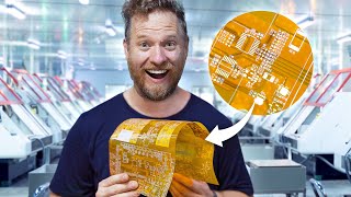
How PCBs are Manufactured & Assembled (PCBWay Factory Tour) - Phil's Lab

Vložit
- čas přidán 29. 06. 2024
- See how PCBs are made and assembled in the huge PCBWay factory in Shenzhen, China! www.pcbway.com
[SUPPORT]
Hardware design courses: phils-lab-shop.fedevel.education
Course content: www.phils-lab.net/courses
Patreon: / phils94
[GIT]
github.com/pms67
[SOCIAL]
Instagram: / philslabyt
[LINKS]
Manufacturing process: www.pcbway.com/pcb-service.html
SMT assembly process: www.pcbway.com/assembly-proce...
[TIMESTAMPS]
00:00 Intro
01:31 Fabrication Data Generation
02:37 Panel Cutting
03:17 Inner Layers
04:18 Lay-Up
05:13 Pre-Pregs & Copper Foils
06:20 Lamination
07:55 Drilling
09:10 PTH & Electroless Copper Deposition
10:13 Imaging Outer Layers
11:54 Plating
13:15 Etching
14:38 Automatic Optical Inspection (AOI)
15:29 Solder Mask
18:24 Surface Finish
19:50 Silkscreen
20:50 Outline
21:44 E-Test & Final Inspection
23:33 Assembly Process & Incoming Quality Control
25:30 Stencil, Solder Paste, Pick 'n' Place
28:01 Reflow & Inspection
29:28 Through-Hole Assembly & Packaging
31:06 Outro - Věda a technologie


Thanks for watching! Sorry about the audio levels on this video. After rendering/upload to YT, it seems the factory background sounds went down to near silent.
It was a BLAST to have you there, Phil!🤭
Thank you very much for inviting me! :)
@@PhilsLab
Very cool being invited to tour the factory. Have many PCBWay PCB's that I've had manufactured over the years.
Definitely was an awesome experience!
We are so happy to have you there then!@@PhilsLab
And after all this I used the wrong footprint.
It's a refreshing video from a CZcams pcb guru instead of generic electronics CZcamsr.
I also work in pcba manufacturing in Europe, have experience in SMT lines for a few years
Thanks a lot for your kind comment!
Fascinating, definitely a process I would love to see in person...cheers.
Thanks, Andy!
Ooh! 31:00 interesting - grey market FPGAs with the barcode and SN lasered off. 😂
Great tour. I love how cost effective and accessible this is for low volume hobbyists these days! Can't believe how much has changed over the years!
A non-technical workmate asked me how circuit boards are made. After like an hour of explanation, I still missed many of these steps off the top of my head :)
Ordered so many boards from PCBway. I was buying boards made in the EU and had no idea how much more expensive they were. £5 in China vs £40 made in Germany for less boards.
There are good reasons to avoid buying stuff from China, if you care think about it. You can buy PCBs from Aisler (Germany) for very cheap too.
Thank you Phil and PCBWay!
It's fun to see the process at the factories that make many of the boards I've designed! I find the chemical specs particularly cool since they're the most removed from what I'm familiar with.
It's crazy how cheap they are able to sell boards for given how complex the manufacturing process is. And with lots of human labor involved.
very cool video. I have seen a few tour videos before but your narration is just perfect
Thank you very much!
Well done!
I was also surprised (like a few others who commented), at the amount of manual labor that seemed to be involved. I was expecting a lot more automation.
I did notice a small thing at about 4:12. You said that for a 2 layer board you would go from step 2 (board cutting) directly to step 9 (Image the outer layers). I think you should have said to go from step 2 directly to step 7 (drilling the PCB). I would assume that a 2 layer board still needs to be drilled and the holes electroless plated.
Thanks for the video, it was very informative.
Nice video! Love to see the inside of this PCB factories!
Thanks, John!
It's amazing that PCB(A) production is so cheap considering the amount of work it takes to produce the boards. I took a trip around several PCB factories in Shenzhen a few years ago and they're enormous compared to anything I've seen in the UK.
Yeah, it's incredible how accessible PCBA has become over the last few years.
Most of our project PCB's are done in PCBway. great vid Phillip.
Nice! Seems like it was a great experience - thanks for the insightful video.
Definitely was - thanks for watching!
Thank you for the tour!
Thanks for watching, Patrik!
Thanks! That was a cool and really enlightening video.
Glad you enjoyed it!
Thank you very much for sharing this video. It would be great if you could create a video on DFM and DFA tips that you learned after witnessing the manufacturing process first hand and conversing with PCBWAY staff.
Great idea!
I'll get a video made on that in the near future :)
Great video.
Thanks, Jeremy!
Thanks Phil. I would have liked to have heard about waste management and recycling. In the west, possibly unfairly, we have a critical view of some Chinese industrial practices.
15:25 - I hope that wasn't my carefully calculated controlled impedance trace she scratches out with a knife!?
Haha I hope not 😅
Pretty impressive video :)
Thanks, Marek!
Lovely.... thanks for taking the hit for us tall people and shrinking yourself into that bunny suit...
Haha sure thing :)
Very cool. I was surprised by the etch process removes the photo mask from where you want the copper then using tin as the etch mask. Wonder what the benefit of the extra steps are over the more common technique of removing the UV mask where you want to etch away? 🤔
Vias being protected.
19:43 after 30sec of silence...a wild "from the manufacturing data" appears lol
I still see a lot of potention for optimisatin an automation so I wonder how they manage theire redicilous prices. But what is very impressive is, the moast machines I saw are actually build by chinese suppliers. I have worked on simmilar machines in europe for half a year and they are very complex.
Hi Phil!
Could you perhaps make a video about creating circuits that are powered via the wall outlet? Most of your videos (as far as I know) only concern USB or battery powered circuitry, but it would be great if you could get into the safety required for using the wall outlet as power supply for circuits.
👍
19:43 there's some odd audio. Sounds like the beginning of your sentence was cut off.
20:45 did PCBWay redact the name of the manufacturer?
Where the audio quickly cuts out? That was bad editing on my part, sorry.
Ni hao
I really can't understand how anyone can endorse PCBWay. They won't even let me upload gerber files to get a quote without entering data first *that can be read from the gerber file in the first place*. Utterly ridiculous ordering process. For a 85cm² 4-layer board, they are thrice as expensive as JLC, and even 20% more expensive than Aisler, who manufacture in Germany. How is everybody so happy with them, what am I missing here?