Classification of Semiconductors (Intrinsic/Extrinsic, P-Type/N-Type)

Vložit
- čas přidán 30. 07. 2024
- While strange at first glance, knowing the classification of semiconductors will help you understand what they are and why they act the way they do. We discuss what's happening at the molecular level in the crystal lattice of the semiconductor and the difference between undoped, or intrinsic semiconductors and doped, or extrinsic semiconductors.
Subscribe to CircuitBread for more videos on intermediate electronics! To see this as a written tutorial, along with helpful tools, go to: www.circuitbread.com/tutorial...
Table of Contents
0:00 Introduction
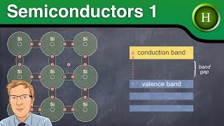
01:25 Pure or Intrinsic Semiconductor
01:34 Doped or Extrinsic Semiconductor
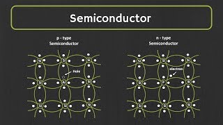
01:47 Pentavalent (N-type) extrinsic semiconductor
02:56 Trivalent (P-type) extrinsic semiconductor
04:09 P-N Junction
04:26 Summary
For electronics tools, tutorials, equations and more check out our site: www.circuitbread.com
And check out our Friends of CircuitBread, who offer special discounts, product samples, resources and more to our users: www.circuitbread.com/friends
CircuitBread is joining the fight to help people more easily learn about and use electronics. With an ever-growing array of equations, tools, and tutorials, we're striving for the best ways to make electronics and electrical engineering topics more accessible to everyone.
Connect with CircuitBread:
Instagram ➤ / circuitbread
Facebook ➤ / circuitbread
Twitter ➤ / circuitbread - Věda a technologie


This five minute video was much helpful than my two hour lecture! Thank you
Same
Same
Samme
Same
same
OH MY GOSH THANK YOU SO MUCH!!! I really liked the way you explained things-it was short, concise and easy to understand. I also liked how organised this was and the visuals really helped as well!! Tysm and I hope you keep doing this.
Awesome, thanks for the feedback!! I'm glad the animations helped!
I WAITED FOR THE TOAST TO POP! But great video! really helping me with my education :D
Brilliant summary, this is gonna help a lot for an assignment
Hi all! I hope this helped clarify things. If you want to be able to read this tutorial at your own pace with the images embedded, go check it out on our site: www.circuitbread.com/tutorials/classification-of-semiconductors Have a great day!
This was so useful for me! I'm studying for my finals and I usually find physics really hard however this video really made it easier for me to digest the information since I was more invested. Thank you so much 😭🙏🏻
Awesome, I’m so glad that this is making physics a little easier!
Thank you so much, this video really does help me a lot to understand much better. Please continue making these educational videos because I NEED ITTTTT SO BAD :'D
BTW, I have liked your video and subscribed to your channel!
THİS İS AWESOME!! thank you a lot. i really loved the video and the visuals. it makes it easier to understand. Keep up the good work!!
Thanks! I'm glad this was clear - hopefully we'll continue to be able to help with our other tutorials!
FANTASTICALLY EXPLAINED!!
very clear and helpful video. Thank you so much
That was AWESOME!!! I was struggling with p type
High quality explanation!!
Hello Sir ,
I am so thankful that I found this video because during this pandemic all that matters is self study .
You explained really well 👍
Thankyou Sir .
Thank you so much, sir. great explanation
Thanks a lot, tomorrow is my exam and I'll bang each and every question related to this topic. You are really a very good teacher 💯🙌💯🙌💯
Thank you for this clear explanation :)
Very well explained. Thanks.
it was very helpful ,thank you
You explain very well. Thanks a lot for this
You are welcome!
Video is very awesome and thanks for sharing your knowledge with us ;)
Thanks Muqaddas, it's my pleasure!
holy shit bud! this video was worth it!
THANKYOU!
thank you si muuch sir for this video love from india
Very calm and interesting
Well Explained. Please make more videos .
helped a lot thank you !!!
yeesss so helpfull, thanks a lot!
thank you best explanation
Valuable content
u are a good man
Thanks Man🙌
Great video btw very helpful!!
Thanks!
Thank you very much
well explained
wow thank goodness found this video
thank you
Thank you
Honestly found this as helpful as my professor reading his slides except you were on fast forward mode. Sure this was a great explanation but this is not meant for the student already struggling with understanding the professors lecture.
Very clear, thank you!!! This will help me for my exams ^-^
Awesome, good luck on your tests!
Hi s3xyy girl
What I like about your video is the precise usage of terms!! Most videos I found on CZcams qualify N-type semiconductors as negatively charged and P-type as positively charged and this is not true (in my guessing )as doping is not about adding charges but instead creating holes and free electrons. Thanks man for the explanation
Hey Soulimane - you're totally right, there will be a charge difference due to those holes or free electrons but that's the result, not the cause.
Fantastic🤘😝🤘
0:34 and 1:50 then 2:56 That's cool! Just FYI (to help viewers) also now _(for trivalent P-Type as in vs pentavalent N-Type),_ Cl doping of Se2Sn (CMOS), so see Van der Waals contacts _(pertaining to Schottky junction/barrier as special case of a p-n-Junction)._
Firstly, thank you sooooo much for your effort and your simplicity explanation, but I need to know something: as we know the intrinsic semi-conductor the p=n=ni; so if I want to convert it to p-type or n-type, how much should I dope with a donor whether with electrons or holes
Oh, I hate this answer, but it depends. You can lightly dope or heavily dope something to and you're usually given a goal and you need to calculate the amount needed. The one thing I can say is that the ratio between the dopant and the intrinsic semiconductor is incredibly low. One dopant atom per thousands of intrinsic semiconductor atoms is incredibly highly doped. Usually it's much lower than that, with one dopant atom per millions or billions of intrinsic semiconductor atoms.
Awesome🥰
Thanks Sanah!
Fantastic! Thanks
Thanks for the vid. I hope you respond, just a little confusion. @ 2:52 it says "an ?EXtrinsic? semiconductor... doped so majority carriers are electrons"... Is extrinsic correct or is it a typo?
Yeah, an extrinsic semiconductor is an intrinsic semiconductor that has been doped. In this case, doped with pentavalent atoms that add "extra" electrons. Am I understanding the question correctly? Let me know!
My teachers should take notes from u ig
Great ...Explanation, Correct me if iam wrong, At 0 kelvin Ptype Semicaonductor behaves as a conductor as there are few holes even at 0 K, and N type semiconductor behaves as an insulator at 0 kelvin
Hi Roshan! Thanks for reaching out - my understanding is that at 0K, all semiconductors (intrinsic, extrinsic, p-type, n-type) act as insulators as the electrons are strongly bonded to the nucleus due to the lack of ambient energy. Even though there are holes at 0K, there still needs to be movement of those holes (which, truly, is electron movement) for there to be current.
@@CircuitBread Thank you so much... Will be watching an add ..to support you..
it was extremely interesting but i still got lost😭
2:29 i cant visualise how there's more p in nucleus than electrons in orbit
didn't phosphorus gain more electrons from Si?
Can i please use some part of this video as a class assignment ? The video is great. I will provide proper credits to your channel.
Of course!
@@CircuitBread Thanks.
Sir, I do have a question! So at 3:40 you mentioned that Boron is negatively charged, so does that mean:
1) p-type semiconductors at room temperature (even when it's itself, say without any contact with another n-type one) are have an overall ionized state with negative boron atoms surrounded by many positively charged silicon atoms? If this is so, then why doesn't a depletion layer form in a p-type semiconductor sheet itself?
2) You said that the holes in Boron atoms grabs an electron from the surrounding valence bands of the Silicon atoms when TEMPERATURE INCREASES, so does this INCREASE mean a temperature raised above the room temperature, or is it just the room temperature? (Hence by increased temperature, you mean any temperature raised from absolute zero)
Also, so many thanks for this amazing video, so far the best one about this topic I have seen!
Hi and thanks for your kind words! Let me see if I can help.
1) Even though the Boron atom is negatively charged when an electron jumps into that hole, the entire lattice as a whole has its charge unchanged. Since it was a neutral charge at the beginning, even though there will be variances within the lattice due to electrons jumping into holes, the overall charge is still neutral.
2) This increase of temperature is basically any temperature above absolute zero, and the warmer it gets, the more likely it is to happen.
I hope that helps - thanks for reaching out!
Thanks for video I understand basics make video on power semiconductor
Can you use yttrium or scandium? For their trivalent electrons
In regards to being trivalent, I believe that would make it theoretically possible if you ignore other factors about these elements. They aren't found in pure forms though and are also good conductors in their natural states, so I imagine those are a few reasons why they're not found in many semiconductors. I'm not an expert on this, though, so I'd be interested to hear if someone has more information about them.
Would you like to tell me how can holes improve conduction of semi conductor
Holes, or the lack of an electron where you would expect one, can help because they provide basically stepping stones for electrons to move around. Electrons can break free of their bond to their atom, move a little, and then drop into another hole. More holes to drop into, the more this electron movement can happen. To keep things easy in visualization and math, we don't focus on that movement of each individual electron but on the seeming movement of the hole.
I don't understand how "most" of the charge carriers would be electrons or holes.....when one electron moves....it produces exactly one hole. It seems that it would always be a 1:1 ratio with no majority or minority carrier. Any help on this is appreciated as I am just getting started, and I am confused. Thanks
That's a very normal question to have, and in undoped semiconductors, you're exactly right. But when you "dope" the semiconductor - add extra holes or electrons by putting in another material - then you get a carrier that becomes the majority carrier.
won't electron current flow in P type ? because as we know that the electron current flow due to free electrons but as there is no any free electron so it means there will be no electron current in P type ?
Hi Aina! This is where it's a bit tricky, as all flow really is the movement of electrons. So electrons will be moving, but we will consider it as hole flow instead of electrons in the p-type material because those electrons will be popping from hole to hole. Besides this hole movement there will also be a few *free* electrons flowing, but there generally will be a lot less than the hole movement.
I always wait for the toast to pop up, like an MCU end credit scene...
😂
Is there have a similarity between semiconductors type N and P?
Actually, other than their dopants, there is no physical difference in the N and P type portions of a semiconductor. To be clear, that's with the same substrate - you can have all sorts of different semiconductor substrates and they will act differently. But then it's the dopant that makes each substrate P-type or N-type.
Thanks for the video ! Just one question, is it correct to say that as the concentration of impurity and temperature increases, the mobility (electron and hole) decreases ? Therefore, as mobility of electrons decreases more conduction exists = electrons jump to the conduction band
Thanks
Hi Roberto! It would be correct to say that the mobility decreases as the concentration of impurities increases. But I would be careful to note that the ability to conduct isn't the same as things actually conducting. Even if there are more electrons in the conduction band, unless there's a voltage potential across it, there won't be conduction. I hope I understood and was able to answer your question!
Wait why is Arsenic's atomic number 4 instead of 33?
does the bread ever get toasted
n type dopoing increases the free electrons as well as the conductivity of the semiconductor AND
p type dopoing increases the holes as well as the conductivity of the semiconductor isn't p type dopoing supposed to decrease the conductivity? 3:52
P-type doping doesn't decrease the conductivity, as it increases the chances of conduction via holes. As holes aren't as mobile as electrons (which makes sense intuitively when you consider what holes actually are), the conduction of p-type semi-conductors isn't as high as a similarly doped n-type semiconductor. But it's still better than an undoped, intrinsic semiconductor.
Excellent 😂
Sir from where the fourth electron comes
If there's an extra electron (or extra hole) it comes from an impurity. I highly recommend checking out some of the other tutorials on semiconductors in our semiconductors playlist: czcams.com/video/n2S7kN12RDQ/video.html
very informative however i think visual learners may struggle to understand like me, as oppose to acoustic learners
Thanks for the feedback, James! I'm more of a visual learner as well, which is why we have the written tutorials on CircuitBread.com - it also gives me more time to go over concepts and let them settle in before moving on. I feel like a salesperson saying it onscreen too much, but we try to encourage people to go to the site as the videos and written tutorials were put together to work in tandem. Particularly with the circuits and microcontroller tutorials.
"In an intrinsic semiconductor material, free electrons are produced when the material receives sufficient *thermal* energy that provides..." why is it thermal energy and not the energy provided from a voltage potential that brings in extra electrons to knock the valence electrons in the semi conductor up to the conduction band? We don't turn on semiconductors with heat... or do we?
We don't actually use intrinsic semiconductor materials in devices (well... we do, but for our purposes, we'll ignore that at the moment). You are correct, though, we do not turn on semiconductors with heat - it is a voltage. But with extrinsic semiconductors, we get more charge carriers because they've been doped and in the case of n-type, those extra electrons literally float around in the conduction band because there's no empty spaces for them in the lattices of the semiconductor. Without that doping, the resistance of the material would be too great and you'd need very high voltages to really do much of anything. Besides that, it's generally the connection of two semiconductors of different dopings (p-type versus n-type or even just different levels of doping of the same type) that make things interesting.
@@CircuitBread I wish I would have seen this earlier - lousy youtube notifications.
ok ok ok, I see where my assumption was about free electrons. It sounds like you weren't talking about doped semiconductors, just the base properties of the materials. Thank you for being so clear and precise about the doping "element" of this topic (hahahahaha). And I take your final sentence to mean the pn junction of a diode or npn/pnp transistors?
Why are they called n-type and p-type? What do those letters refer to?
Great question! I may have knew this at one point but I had to look it up again. As electrons have a negative charge, having more of them makes a material n-type. Holes (or lack of electrons) makes the material have a more positive charge, making it p-type. N-type for negative, p-type for positive. Makes sense to me.
I wonder why we need to increase the conductivity of a semiconductor by doping it, while we already had conductor (metal) for that purpose?
Hey Son! That's an excellent question. It's all a matter of scale. Even when the semiconductor is more conductive, it's not as conductive as metal, on purpose. You still need a bandgap in the P and N materials to make a useful PN junction, otherwise you'll just get an ohmic contact or a Metal-Semiconductor junction (useful in certain applications but not others).
I think the best analogy that I can give is the water pressure on a faucet. If you want the pressure to be at maximum level, you would open the valve fully. Same with conductor, if you want the current or voltage to be at maximum, you’ll probably use a material with the smallest resistance which would be a conductor (metal). But if you just want the water pressure to be low, you would just open the valve a little. In semiconductors, doping acts like the valve, which allows you to control the current or voltage just like in a transistor that is configured as an amplifier.
Didn't realize you're a Bronco!
different element have more covalent bonds for a first time listening
Trust me or not , but told us a 5 page theory (with no surety that if we understand or not ) in a 5 minutes video (which we fully understand)
Glad it was helpful!
Speak some audiobook dude
Haha! Thanks, I'm not quite sure what to say to that 😄
Yeah this guy is right your voice is so clear
😢porque no está en español
Nos encantaría traducir todo a español (y otros idiomas) porque unos de nosotros en el equipo hablamos español (no muy bien, pero bastante bien) pero cuesta mucho traducir todo...
طالبة سادس من العراق تحاول فهم الموضوع اكثر🌸😅
Well, I hope we can help! Good luck!
وياج نفس الحاله
P type doped with B not the N type as u mentioned
Could you provide a time stamp? At 3:03, Boron is mentioned as a trivalent atom, which makes it a P-type dopant. Not sure where we said that it was n-type?
@@CircuitBread i was drunk sorry
😂
You are too fast, please try to slow down. But nevertheless it was helpful.
You are so fast😭😭😭😭
You can slow down the video from the settings
Boise State!