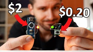
This credit card sized PCB can SAVE YOUR LIFE! (Shrinkify your projects with a 4 Layer PCB)

Vložit
- čas přidán 17. 05. 2024
- One Stop PCBA, Get $24 SMT Coupon:jlcpcb.com/AAA
Get my PCB design & Name Card Gerber: bit.ly/3tNjXji
Free Altium Designer Trial: altium.com/yt/greatscott!
Previous video: • New Supercapacitors wi...
Box project video: • A Box that can SAVE YO...
Facebook: / greatscottlab
Twitter: / greatscottlab
Instagram: / great.scott.lab
Support me for more videos: www.patreon.com/GreatScott?ty=h
More project information (code, schematic, pictures,....) on Instructables & EasyEDA: www.instructables.com/A-Box-T...
oshwlab.com/GreatScott/smscal...
Parts list (affiliate links):
Aliexpress:
1x Arduino Pro Mini: s.click.aliexpress.com/e/_APsmG8
1x A6 GSM Module: s.click.aliexpress.com/e/_98ih6y
1x NEO-6M GPS Module: s.click.aliexpress.com/e/_A5Pys4
2x Slide Switch: s.click.aliexpress.com/e/_99gyF2
1x Tactile Push Button: s.click.aliexpress.com/e/_A3GIVQ
1x TP4056: s.click.aliexpress.com/e/_dX8...
1x LiPo Battery: s.click.aliexpress.com/e/_996Mx2
Amazon.com:
1x Arduino Pro Mini: amzn.to/3D0YFiM
1x A6 GSM Module: amzn.to/3D1bdXN
1x NEO-6M GPS Module: amzn.to/3D2hpyB
2x Slide Switch: amzn.to/3DZRpVO
1x Tactile Push Button: amzn.to/3FThzdn
1x TP4056: amzn.to/32FcNC6
1x LiPo Battery: amzn.to/3refAfN
In this video I will show you how I turned a big and clunky electronics project into a rather small form factor that can easily be carried around. The project itself can call your phone and send an SMS with GPS information. The new credit card sized PCB version can do all of that while being way smaller. The reason is a 4 Layer PCB design which I will tell you all about during the video and how you can make your own. Let's get started!
Useful websites which were shown/mentioned in the video:
www.electrodragon.com/w/GSM_G...
www.smart-prototyping.com/ima...
www.makerfabs.com/wiki/images...
www.electroschematics.com/neo...
wiki.sunfounder.cc/index.php?t...
Thanks to JLCPCB for sponsoring this video.
Visit jlcpcb.com to get professional PCBs for low prices.
0:00 My old project is TOO BIG!
1:26 Intro
2:08 Component sourcing
3:16 Creating the schematic
4:25 4 Layer PCB design
6:48 Soldering the PCBs
7:55 First test & troubleshooting
9:08 Final Test & verdict - Věda a technologie


I think this board could be possible on 2 layers. Use old laying technique: vertical traces on one layer, horizontal on another. You can fill empty space with GND and apply via stitching.
2 Layers is possible. I tried it. But I thought it was time to talk about 4 layers ;-)
I never knew about that technique
@@YSPACElabs Very useful when you have a lack of space, just be careful when you have high current traces or AC. Parallel lines can easily act as antenna's.
@@YSPACElabs often used on old computer designs with a lot of discrete parts, I still use it occasionally when I do my boards
Yeah but then you can't get that sweet sweet jlcbcb money
I enjoy the fact that you like to revisit old projects. Showing that even the very experienced go through varying versions of a project.
Also, that you like to share your troubleshooting. That, in and if itself, is super useful.
Thanks!
Thanks for the feedback :-)
The 328p is quite easy to use on it's own and saves a lot of space not having a whole arduino. I've made projects using a 328p that ended up smaller than a nano.
Basically just a single pullup resistor if ur fine with the 8mhz internal oscillator. Otherwise +2 caps and a crystal
@@KekTekDe And an ICSP header or pads. They're a very useful MC
or we can ditch the venerable 328p and use a RP2040 :) (although if space is an issue, the bare 328p with internal 8mhz is hard to beat)
@@AudreyRobinel well, for this project an attiny would be sufficient 😄
@@KekTekDe Well, it may be suffiscient, but modern micros are as power efficient, and as cheap, providing with greater flexibility, and easier code maintenance :) why pay the same price for a lesser technology? 328p are not significantly cheaper than rp2040s and they are outclassed on most, if not all metrics!
Interesting project. Great work. This year I had to design a six layer PCB at work and it was a daunting task at first but ended up enjoying it.
I think once you get into designing it becomes like solving a maze. And I think that is quite fun and challenging at the same time ;-)
@@greatscottlab Yeah it can be very fun trying to fit all the parts and make the layout as efficient as possible.
@@akhurash How is this comment 6 days ago :d
@@bkaytan patreon get early access
@@greatscottlab very true until you use........................... the AUTO ROUTER haha. on any design with some complexity it requires a lot of hand holding to get the auto router to do its job.
Create a raised ring around the button so you don't inadvertently press it when sitting down or leaning against something.
there's an on/off switch independent of the button
@@Astarath It's still a good idea to protect the button, just as it's a good idea to protect the slide switch.
Great video. You could have desoldered atmega chip from Arduino board as well, as you could get even smaller circuit. Arduino is anyway mostly atmega plus usb-to-serial chip and oscillator which can both be avoided in some cases.
True, and the pro-mini doesn't even have the usb-serial chip
As someone with social anxiety, this is a godsent project.
Keep in mind that RF traces (like the one going from the GPS to the antenna) need special care and should be kept straight and some other things like the length need to be precise.
Yeah. It's a miracle that it even works. It needs to be short and FAT. GSM is another thing, it usually works with a wet string, but it might be noisy as hell. GPS on the other hand is really easy to screw up.
shouldn't they be controlled impedance traces? 50R?
Not if you are using active antenna. It seems he is using a active antenna, which is fed with a small bit of power, meaning the conductor between antenna circuit and GPS circuit isn't critical, but the conductor between antenna circuit and the actual antenna is critical. The antenna circuit is on the board where the antenna is mounted. An active antenna is ALWAYS required when connecting a GPS to any length of antenna cable, since when using passive antennas, you get reflections and such in cables that can disturb the sensitive GPS signal.
@@sebastiannielsen you also get impedance mismatch and reflections with a LNA. No way around that.
@@zaprodk Yeah but then with the amplified signal back, the SNR will be higher, meaning it doesn't matter if you get some crap on the line.
This is just beautiful.
Going back to redo old projects and make them even better is such a cool way to go about DIY
I was always thinking what are those small holes in the PCB's. And now i know it. Thanks for answering my question.
Glad I could help!
I like the new intro reel more than the old one. It is perfect amount of length.
Now you can keep track of every chair you sit on. Great project!
Great tutorial as always! Since 2G networks are almost all shutdown in the US, it would be awesome if you did a similar project with a LTE module such as the SIM7000 as it also has built-in GPS.
The activation button should be recessed to reduce accidental triggering from clothing. You don't want to be butt dialing. Also I would consider requiring 2 buttons that have to pressed at the same time.
I thought the same, and perhaps recessed dip switches as well. I bet the enclosure could be made half as thick.
I believe there are 2 buttons, the switch must be activated for the button to work.
don't kink shame people randy, maybe I do want butt dialling!
Loved this video because you covered some good points and challenges of designing a pcb! You should do more like these!
Going through data sheets and pairing up components is hard but so satisfying when it works.
Here is a very good project.
I even see an evolution;
Imagine an elder working in his garage and unfortunately he falls and has trouble getting up.
With some modification your system could send an sms to a list of people selected in "help me" mode
Very nice video as well as PCB design! We love it and we're glad that you're happy with our service! 🥰
Delivered exactly like I asked for, thank you for the video and the hard work!
I love your videos. I just ordered my first PCBs for a project about a week ago. I will definitely be designing boards for future circuits.
There’s still a lot of wasted space, though, almost half is taken by the Arduino, the switches and the button. By using an SMD microcontroller directly on the board, an SMD button and switches (or removing one or the two switches) and a dual GSM+GPS module, it probably could be shrunk to half the size or less.
Maybe he can make a version 3 for us
@@whizzbang7520 I'm kind of trying to minimalize the design right now with a fork of that project. Fixed the mess in the schematic, put all in blocks so it's readable and debuggable. Get the routing done without the godawful autorouter traces. Also wanted to find an enclosure that one could buy already done from a manufacturer, that would be small and easily modifiable and they have CAD stuff, so people with 3D printers can waste their plastic too if they choose. The Ai thinker A9 has GPS and GPRS so could use that later, but for now, because this project also has the code for all the stuff here, I would not try to change much but just the PCB.
@grbttutorials Please post a video of making this project even smaller
@@deskpro256 can you link the release when its done?
Very cool...never thought of using a 4 layer board w/ the gnd and vcc planes like you did...that will DEFINITELY make things easier to route!
Keep em coming!!!!
Maaaan that's such a great example of multi-layered PCBs! Gotta love the enthusiasm of the outro.
Awesome channel what really draws me in is you buy products then build the same product then give us all the results good or bad ..keep it up ..as a mechanic with an electrical engineering certificate I really learn a LOT from you and can see a LOT of places in vehicles where Arduino can fix issues like factory problems or after market modifying or discontinued ancient stuff like 1980s Mazda's I own ...
I once worked making software to a company that could make PCB boards with more than 20 layers. Never found out what special applications those insane boards were for, but it was quite impressing. I heard that the amount of rejects was quite high with those PCBs with all the blind holes and holes between layers deep inside etc.
wouldn't be surprised if smartphones and pc/laptop mainboards are about there.
@@victortitov1740 No. Smartphones and pc/laptops will propably in the future go to a common bus architecture, meaning they could be done on 3 or 4 layer boards. Today we still have HDMI ports and such on laptops, which require its own circuity, but in the future the whole laptop/smartphone might just consist of a single USB-C bus + power + gnd going around every component including storage and processor. And with the new RAM types that can nonvolatively store data, I think we in the future will use our RAM sticks as harddrive.
How I haven’t seen this awesome channel before is beyond me. Definitely subscribed
Engineer before work: clean and tidy
after work: messy af
I am new to pcb and I learned a lot thanks
Wow! You made this look so easy. It inspires me to try something like this as I too have a similar wireless project in mind. I also have never done anything like this before so there will be so much to learn.
Fantastic work, dude! Nicely done! 😃
This project was great, but it's even better now!
Anyway, stay safe and creative there! 🖖😊
This is amazing. I've been looking for something like this for a few months. Just my big doggo and I these days and it kinda scares me as I get older. Thank you for sharing this.
Hey scott! I love that you revisited your old video and solved the problems. And just asking, can you start a series of arduino programming which you discontinued years ago? Because I love your videos and you are a great teacher too! Hope you will start the series...
Love your projects.
It's a very useful project !! Every senior who lives independently should use one of these, and even people who live alone and can be robbed are an important solution !!
Thanks :-)
Nice job! Thanks for sharing.
Wow. The circuit is beautiful and complicated at the same time. Really amazing work.
Thanks a lot!
Thank you for the amazing videos! very useful and informative while still being fun to watch
This is the first time I saw great Scott on video. Mashallah a good looking man.! May God guide you always.
Great video! I think my next PCB also will be 4 layers, as JLCPCB really has made it affordable enough now. I am not sure if I liked the close up at 10:04 though. Loose solder balls or flux residue, I am not sure what that was, but if I see things like that in my own projects I usually flux and run the iron over that another time and clean up before I call it 100% finished.
Nice to see someone using 4 layer pcb :)
Glad you like it!
Impressive stuff sir! Seriously!
🔥 content #GreatScott keep doing your thing
I’m loving the new intro!
Nice, this project now is 4 boards shorter than first version! 😉 Now it's more practical..
Great video, as always! 👍
Excellent pro job! Congratulations GreatScott! Also the smile DAMNED 01:23. Now you could waterproof the box because there are plenty of floods in Germany! the box can prove useful for survivors.
So much to unpack. Great video. Thanks!
Really nice work!
"4 layer" I'm still at single layer home etched... Man I need to catch up to the rest of you 🍻
You will get there ;-)
Truly awesome
Your brave. Good work
I had been working on making a diy 2 layer pcb and now scott post a video- awesome!
Hope you enjoy it!
I run a hardware business and the chip shortage has certainly changed the game quite a bit. We've had to build up a bunch of chip inventory management and ordering processes to ensure we get what we need, along with accelerating board redesigns.
Chip gougers like Win Source are a blessing and a curse. They purchase chips and markup by nearly 10 times, but at least it means you can get your hands on chips for prototypes.
Have you ever bought from Win Source? Hard to tell which ones are scammers or not.
Very cool project!
that new intro is pretty swag ngl
Love the new intro!
As a newb just learning about the metal stencils I'd like to share with you more experienced guys how freaking cool that is.
wonderful, keep going😄👏👏
Very nice video. You don't always have to come up with fancy stuff, so how to design a pcb even though with 4 layers is very condense. Keep up with the great work!
Ps: always fascinated how easy your debugging looks like :D. I feel like I need days until I find the error
Cool board! Although I'd suggest swapping out the GSM module for something lower power though. I bet this thing eats through the battery charge like crazy.
There are plenty of LTE modules out there that are cheaper and lower power, and oftentimes have integrated GNSS receivers. Plus, with 2G network shutdowns happening globally, this could stop working in parts of the world.
Nice concept though!
Cool project the chip shortage sucks but you harvested what you needed.
Nice job!
I think rounded corners all around the outside of the box would make it better to carry even in a bag or backpack, not to mention pocket.
Like most of your videos. Great Scott
Your project are very interesting and I want to be a student of you...Scott sir
Thanks for the video
you are a genius
Loved the video. Great Job! And you had not even ONE dislike :)
only on a nerd-channel we are talking about the details in depth of a box that gets you out of a conversion, instead of improving social skills xD
very well done as usual
Lot's of good information. Way to go!
About the Auto-route, for me, it's ALL about attention. Check, re-check, three-check the connections, especially the data lines, and you usually save a lot of time on medium/big-sized boards.
Well said!
That was awesome 😀
I was waiting for u💗💗💗💗
Very interesting video, I have always thought it would be impossible to make a 4-layer PCB with my experience (almost none) but it just took time and in some cases it was easy. Thank you for your informative content (:
The usual practice is to make the interior planes on a 4-layer board the power and ground and run all the circuit traces on the outside planes. This means pesky blind vias for everything that needs a power supply, but you're going to get them anyway and this probably produces the fewest in most designs. With that in mind, designing a 4-layer board is probably going to be easier than a 2-layer board, if you've done a few 2-layer boards.
If you move the switch and buttons to one side, then you could make the whole PCB slimmer which would be more comfortable in your pocket and then could be inserted into a pocket of a purse or handbag. This board could also be used as a GPS tracker enabling you to find the unit simply by sending a SMS with a code in it, which triggers the GPS result in a returning SMS.
Genius!
It is very useful and is certainly marketable especially if it were smaller and more inconspicuous.
Great video! Looks super cool compared to previous bulky version. Going to make it. 👍👍
Have fun!
Maybe a community tab upload, but I would love to see a photo of a side-by-side comparison of the old enclosure vs new one for scale :)
Oh a new intro!! I love it, had to admit i really disliked your old one for years :D Yet another great video of yours!!
Great 👍Scott !!!!
JLC pcb =perfect
Nice work! I like this project
Thanks!
Brilliant
Another awesome video from great scott 😍
Glad you enjoyed it
Good job, I like the way that you working
Glad you like it
You should definitely make this a full product you can sell !!
I like the new video intro!
Great one.
For such a project I would be worried about radio or other interference among the components because I don’t know about such things but do know it can occur. It’s awesome that it worked!
Yep :-)
With two-layer boards I make one side GND and the other VCC after the signal lines. This even makes a small capacitor.
OK, awesome. Now make a more useful one. :)
Two suggestions:
A motorcycle tracker that cries for help if the rider doesn’t silence/acknowledge an alarm within 15 minutes of it regularly going off. You know: SMS, email, etc with GPS coordinates and an eventual call to emergency services with a pre-recorded message + last known coordinates.
A camera that emails or sends MMS thumbnails when it detects motion as well as providing a live view when you request it remotely.
The later would preferably be activated as a backup when there is a network or power interruption to your non-GSM cloud-connected cameras (Nest, Ring, etc) or when you specifically need it… like you position outside with no power source to capture a trespasser, for example.
Oh my god, what a wonderful video, i respect your effort.. thank you
Glad you liked it!
i am really excited to see the new studio wiring video with german standerts and hager stuff!!
That will take a while though.....
It might be useful to have a safety switch to save from the inconvenience of but dialing as the button is quite noticeable in pocket, great idea either way.
I want to make one of these!
I cannot wait when you gonna use the 6-layer PCB. Great video as usual :D
Maybe in the future ;-)
Love the new intro :)
Drinking game: Take a shot every time you hear "And just like that".
Nice video, like it, thanks for sharing :)
GS, Love your vids! Curious as to which microscope you are using?
Un buen sistema de emergencias, un saludo amigo.
Turning this project into a watch or a keychain would be an excellent next step. Even better might be a mode you can set it to to send gps co-ordinates to someone on an interval until the battery dies.
Genial video, siempre los veo todo un pro gracias
Hey man I just recently started getting into electronics and this type of stuff but I just want to know if through the hole components are still used, because I’ve seen a lot of SMD but I just think that would be a little difficult for me to start with, plus I already have a really good Weller iron I got for Christmas and I really want to use it for projects, also just where do I start to get into electronics