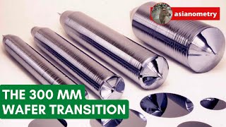
The Amazing, Humble Silicon Wafer

Vložit
- čas přidán 31. 05. 2024
- Silicon is probably the single most studied element on earth. Over the past seventy years, people have researched more ways to cut it, etch it, grind it, clean it, crystallize it, polish it than almost anything else.
Engineers have done amazing things to turn this plentiful shiny rock into the century’s most impactful piece of technology. And the wafer industry needs some love for those achievements.
So in this video, we are going to talk about the decades of research and stunning engineering that have gone into creating today’s cutting-edge semiconductor wafers.
Links:
- The Asianometry Newsletter: asianometry.com
- Patreon: / asianometry
- The Podcast: anchor.fm/asianometry
- Twitter: / asianometry


Hope you enjoyed the video. Check out other deep dives here in the playlist: czcams.com/play/PLKtxx9TnH76RiptUQ22iDGxNewdxjI6Xh.html
I just want to thank you for yet another very interesting video. 🙏
@Asianometry you seem to have found the right idea for your april 1st video :-)
man this is epic now I know how cpu is so important
@@masternobody1896 and you haven't seen much yet... It's barely blowing on the surface.
@@leyasep5919 lmao then tell me
I hate it when I accidentally dip my pen in to a crucible of molten tin
Happens all the time
@@Asianometry I happen to have a crucible with molten eutectic tin+lead to help when I must "tin" a lot of wire ends.
I'd have to be very very tired to mistake it for an ink reservoir.
Czochralski czochrał his pen in the wrong crucible... nothing out of the ordinary for him... 😆
8'957'656th invention due to a mistake.
'make it look like an accident' :)
"Like all minerales and people, quartz is influenced by the enviroment in which it's grown". So double true. 👌
Deep
"Paper is an Ipad that doesn't run out of battery."
Don't know why, but this seems more deep.
@@Dr.Kraig_Ren I freaking died. Absolutely lapped up whatever the hell that was.
@Dr.Kay_R Ikr, paper runs on green energy.
as someone working at ASML I scream internally when I see those wafers out of a cleanroom and someone touching them barehanded.
but they look SOOO GOOOD !
anyway I feel for you.
Harder, better, faster, stronger. Can't believe they split.
:(
Damn dude why would you remind me out the blue like this.
One more time, a celebration
You know we're gonna do it right
DID THEY??
Its hard to think that they could have kept going after RAM and Electroma come out. That really seemed to be it for them. No more nostalgia for the duo as just that.
0:06-0:09 are the best 3 seconds of a technical video ever
I want to see him rap in his video.
0/10 video needs more demonic mechanical babies.
DO IT MAKE IT HARDER BETTER FASTER STRONGER
Loved the dry humor of that pen joke.😙👌
"Paper is like an iPad that doesn't run out of battery." Wow, that's amazing, I wonder why Apple makes iPads instead of paper when it doesn't run out of battery.
well, Apple can control what you install, do, watch, pay... Paper is too liberal :-D
Ibm made a paper think pad. Definitely superior to the ipad, and much cheaper to produce. It's a shame technology is getting worse.
@@gunner75171 oh, was that an April fool's joke ?
Then they cannot charge you for battery replacement.
The problem with paper is that it has a high per-frame cost as it is single use only and that it has a high display latency when a printer is used to update the screen or when a the display is manually scribed with a piece of graphite.
Always blown away by the research and numbers here. Would love to get some insight on the research process behind these videos
His research process was covered on episode 24 of the Compounding Curiosity podcast, by the way
@@shazmosushi thanks for a great recommendation
@@shazmosushi thanks for the info.. Just downloaded it
my father designed machining for intel for board assembly and placing silicon wafer. said at the time it was almost impossible to do at the scale and had no clue how it pulled it off. He didn't even understand the engineering he did, but it worked. This was in the 90s. He still keep parts of the prototype around. Kinda cool.
Sounds like how we get tracked by Meta even without knowing how they track us. _(By the way, Meta is just a Facebook with a M instead of F)_
( ͡° ͜ʖ ͡°)
@@Dr.Kraig_Ren "without knowing how they track us." pretty much every web developer, of whom there are literal millions, know how facebook tracks users, it's nothing marvelous. Bosses of millions of different websites that help facebook track your presence literally ask their hired web developers to plug in tracking scripts from facebook. It all kinda started from the Facebook like button that at some point had spread the internet. Even though this button disappeared the scripts are still used only that more often now they are hidden. Website owners plug these trackers because it helps them make few extra bucks from advertising partnerships.
-at 2:43, it is pronounced "peg-muh-tight" that they mine the quartz from. Pegmatites are any rock with very large crystal sizes. -Geologist
It isn't an Asianometry video without a mispronunciation.
Just wait until you get a Polish person watching this.
It would be nice to have a video on the industry of solar panels
I did a video on the Chinese solar industry a while back. Worth checking out
yeah let's talk solar valley rather than silicon valley!!
“Paper is like an iPad that doesn’t run out of battery” -Asianomotry, 2022
You might not believe this but I worked at a company in the 90's that got a job from Sanyo Solar in Carson Ca. (LA county) to make ingot transfer carts for ingot right out of the growing machines. They were lined with 1/4" (6.25 mm) kelvar blanket material. They made Solar panels here in the US! Or at least the silicon wafers. That was a different era. Paying people a bowl of rice for a days work became the trend.
Thank you for this. I finally got an answer for why wafers were circular if it was obviously more efficient to print square chips on a square substrate
It would be less efficient actually. The optics is round, so you would just lose part of its field, not get. Square substrate would be not only more difficult to get and process, it would be impractical for cleaning, where you need to rotate them. The corners would be more susceptible for damage and cracks. Square substrate is bad idea on so many levels.
Problems would be created for the spin coaters which spin on etch resist on the wafer with a square wafer.
Gen-Z-splaining pen and paper was hilarious
Standing ovation Sir! And it's a miracle that you didn't break your tongue at the Polish guys name! :P
He did poczochrał Czochralski name and made Czouchralski out of him. :P
Gonna bet that he used google translate to read it because google translate is reading it as Czo-chra-lski,
voice sounds like a native Polish speaker but in 3 separate files.
btw.
"czochrać"= rub, tatter, tousle, scratch, ripple. But most of the time you can hear it in Poland via word "poczochrany"(for man) or "poczochrana"(for woman) when someone is trying to describe a mess of hair, so i am not surprised that Czochralski invented his metod by messing of the pen...
I actually found a YT video of Polish guy to figure out how to pronounce his name correctly: czcams.com/video/Qg48Xe6U5qs/video.htmlsi=FUDlfES9ilYAgFEh&t=85
Jan Czochralski is currently the most cited Polish scientist all because of an accidental revelation. The method is probably semiconductor's equivalent of penicillin and just as much crucial.
I used to work for a semiconductor company. And was once given the opportunity to visit Shin-Etsu in Japan and see their production line for SOI wafers. That was a great opportunity as I have now seen the entire manufacturing process: seeing the production of wafers, visiting a wafer fab, and have visited assembly and test sites.
0kll
I definitely want to visit Soitec one day, their SOI manufacturing process seems really cool.
Gallium Arsenide (GaAs) were considered to be the future in the 1990s. They are still around as a niche product. Another niche is Silicon Carbide (SiC) for power electronics.
And now molybdenum disulfide is showing up for power electronics, though currently on smaller stuff like 45w chargers. I don't think any cars or chargers for cars or forklifts have used it yet. There's potential to make it useful for logic, but there's a lot of work to be done in order to make it so.
@@Jaker788 are you sure about that? Power semiconductor technology is my field of expertise and I have not heard about any research into MbSO2 I would be interested if you can point me towards any research you are aware of
I worked in the 90's with both GaAs and Si.
GaAs logic devices were much faster but the yield rate was diabolical. If I recall it was as low as 50%. That and material cost meant it was just far too expensive to be used for commercial grade chips.
The metallisation layer we used was gold, so no doubt that made GaAs more expensive.
I remember doing one design and the engineering samples (a small pre-production quantity) cost £1000 each, this is 1990's prices.
The common joke back then was that GaAs was the semiconductor of the future and always would be.
@@deang5622 So basically silicon is a poor man's material? :|
the freedom units at 9:30 hurt my soul
🇺🇸🇺🇸
That pop music intro though...
Appealing to the youths
It turns out we are so good at fabricating silicon, and have such a close understanding of the properties and isotopic distribution of it, that we now use it as the physical translation of the new SI kilogram.
Silicon is awesome, and there was a project to make an exceptionally round 1 kg sphere of isotopically pure silicon. But that is not how the kilogram is defined. The modern definition of kilogram (in force since 2019) is based on "Kibble Balance" -- a special instrument which reproduces kilogram based on the value of Planck's constant and other fundamental physical units defined through their respective standards.
It's not the basis of kilogram.
Kilogram is now defined using universal constants
@@cogoid sorry, I was less than clear. I am aware that the kilogram is defined by Planck's constant, but i was referring to how we have used our exceptional knowledge of silicon as a part of checking that process.
You did a great job describing the Cz single-crystal-silicon ingot pull ;) I worked at ARCO Solar a few years, then Siemens purchased ARCO. People don't realize or appreciate the amount of energy and effort it takes to grow an ingot. The melt of silicon on the crucible is rotated say, CCW while the seed is rotated CW. The seed is oriented a specific way ( the term 1-1-0 rings a bell ), and as I recall 4mm x 4mm x 100mm. I was there when we changed from ID saws (more kerf loss) to wire saws (the carbon slurry was with Mobil One) We could cut 4 ingots on one wire saw, yielding about 800-1200 wafers per 36 hours where the ID saw took about 48 hours for one ingot yielding about 200-250 wafers. We made 105mm wafers (as I recall), then 125mm after I left.
This is what is great about the internet, thanks Jon. Knowledge of how our world works, well presented, easily referenced.
Growing up my mom used to work in a fab in SoCal and she would sometimes bring wafers home and show me what it is she did for work (I was a kid, had no clue wtf she was saying it was way too complicated). I'm guessing the wafers she brought me were faulty orwere thrown out for QC issues since they seem kinda expensive.
Her company (Microsemi) was snapped up by an Israeli firm and she switched industries shortly after. I have so much respect for her, can't believe humans went from cavemen to turning sand into these hypercomplicated semiconducters. If you tried explaining this process to someone not too long ago they would just chalk it up as being magic.
Hi, enjoyed the Wafer video. I worked at a (at that time) Monsanto Silicon Wafer plant in Spartanburg SC. we built a new plant there and made 4" and 5" wafers. At that time (early 80s) that was about the largest being produced commercially. I actually have quite a few samples, lapped, polished as well as a short piece of rod and some chunks of polysilicon from a quartz crucible, actually have a couple of those also. Was a great business, but moved on in my career to other businesses.
“Paper is like an iPad that doesn’t run out of battery” 😂
Great video 👍🏾
Had me dying!!!🤣🤣🤣🤣🤣🤣🤣
He roasted gen Z to the Bone... Lmao
The funny thing is he's probably right. Imagine gen z looking at vacuum tubes.
@@KarrasBastomi ok boomer
@@hotosabjatahaiprabhoo..kar8081 Easy there, we are just as much ok boomer as you are. It was one hell of a joke.
The sheer complexity of all this going into the first IC’s (nevermind subsequent advances) makes me terrified of how much knowledge would be lost if there was ever a significant disruption to civilization. Back to boolean gates and relays, assuming you even have enough population density and law and order to justify the effort.
Relax -- look for "I, Pencil" by Leonard Reed (I think). A page or so, and there is at least one video of it. It's all about how no single person knows how to make something as simple as a pencil, once you get into the chain saws to cut down the trees (who makes them?), the mines, the ships to transport everything ... in effect, if civilization collapses enough to lose the knowledge of how to make integrated circuits, it will probably also lose the ability to make even pencils. No halfway collapse, it's all or nothing.
There was one person who actually did try to make a pencil from scratch. I think it took him about 8 months, and that was with a lot of short cuts. It's a fascinating study in what we know.
GenZ approved ✅
7:01 --- HAHAHAHAHAHAHAH AHMAZING
I'm an old American koot of 62, I was working in the burgeoning digital and mixed signal industries in California in the late 70s though the 90s I enjoy this channel greatly. It saddens me to see where we have fallen to in America even with the luxuries we now enjoy from the brow sweat of our patriarchs
Silicon wafers are my most favorite snack.
the gen-z shade, lmao
Best video ever. Extremely informative, and the purity of the memes is off the charts!
I find it amazing that an entire supply chain + production process that is less than a lifetime old has changed the way every human lives.
Daft Punk sends their love.
YEAH! I caught that too. I think I only caught that because I just listen the 2007 Alive album.
This probably won't be your most popular video but its incredibly important. I'll have to do some reading on US domestic silicon boule production. It seems odd that we would be financing a $12bn TSMC plant in AZ while also having the source silicon produced in the US without producing 300mm wafers here as well (we very well may, I just don't know).
If you're running low on ideas, electron beam lithography has been able to produce nanometer(ish) feature sizes for almost 30 years. I know the DoD has been funding it for at least that long but I don't know what secret squirrel types of products have been being produced by EBL.
-edit
Oh, also, yeah... Graphene. A lot of people (not you, other people) make the mistake of thinking a good semiconductor is automatically equally good at things like forming insulating layers or accepting metalization layers. Decades have gone into developing dielectrics and processes explicitly for silicon that are completely incompatible with graphene.
Lets go full TL;DR. Graphene might be another good topic. I'm assuming that semiconductor grade graphene has very little to do with the idealized graphene sheets people think of. I would think it would have to be at least cross linked graphene. I don't think you can just stack a bunch of graphene layers on top of each other and expect them to stay stuck together through even just operating temperature differentials.
Also: high-k dielectrics. That was on the radar like a decade ago at the 45nm node, but everything seems to have gone quiet. I don't think its because things are actually quiet though. I think high-k dielectrics are now very highly guarded industrial secrets.
EBL is used to make masks for photolithography.
As someone just beginning to fall in love with the world of engineering and electronics this video was fucking phenomenal thank you
then watch the whole archive of this channel.
Then find other channels, CZcams has many electronics design specialists !
the subtle references at the start of your videos are amazing
Thanks, there is a specialty producer in Southern Oregon as well producing silicon wafers for specialized applications.
omg, i LOVE LOVE LOVE these silicon wafer vids!!!! keep the comming!!!
(7:02) LOL, indeed: I did learn to write with that back in elementary school.
Great video! Heavy on the jokes...
The silicon demand problem isn't solved by graphene either. Graphene nanoelectronic devices still require a silicon substrate. Graphene is useful when it's as flat as possible, silicon, more specifically silicon dioxide, is not flat, but provides a good starting point. Atomically flat flakes of other crystals, Hexagonal Boron Nitride (hBN) being one, are placed atop the silicon substrate. This is achieved by peeling off thinner and thinner layers of hBN crystals from a larger parent crystal. Graphene is then transferred onto the hBN using a similar method. On the hBN, graphene can lay falt and it's tremendous properties can be utilised. So although graphene is an interesting and exciting advancement for nanoelectric and spintronic devices, we're a long way from a silicon free world. Silicon itself is too versatile a substrate and the manufacturing processes are too well developed to transition to other materials just yet.
If you're interested in more, check out the Graphene research group at the University of Manchester. I used to work in the condensed matter research team there under Dr. Ivan Vera Marun. My research involved investigating magnetotransport and thermoelectric effects in ferromagnetic channels on hBN substrates. It's cool stuff!
what "silicon demand problem"?
Thermoelectric effect - cool stuff. Loving the pun Mr. Owens 🤪
Struggling to remember now, there used to be a materials science building, was it a joint venture between Owens and UMIST I think?
NICE #DAFTPUNK REFERENCE
I wasn't paying attention for a short time until I heard you say, "paper is like an iPad that doesn't run out of battery!" You get a video like from me for this.
Cut it, etch it, grind it, clean it, crystalize it, polish it.
Technologic.
Technologic.
In the category of alternative materials to silicon, unmentioned are diamond (carbon) and gallium arsenide. There was also a vogue for sapphire as a base material (coating of the wafer prior to patterning), which if this old man recalls was SOS or Silicon on Sapphire.
I feel like we're glossing over the detail about Czochralski keeping cups of molten tin on his desk
Maybe he simply liked to czochrać in this molten metal form time to time?
Instructions unclear, paper ran out of battery...
Love the information and tidbits of humour!
I love the primer on pens.
ABSOLUTELY MINDBLOWING! What's even more amazing, considering the modern miracles of science which goes into creating these microchips, is that one microchip doesn't cost as much as a house. If you were to travel back 100 years, you wouldn't even be able to explain the concept of a microchip to another person. It would have been far beyond what even science fiction was capable of imagining. To the untrained brain, mine for example, just one microchip is as mind-boggling as the depths of the universe.
I think the thing I learned the most from this video is what is pen and paper, none of my classmates know
Tons and tons of information that I could not find in any other video tutorial. GREAT JOB! Thanks!
You left out Gas Plasma Vapor etching. It was big back in the late 60's and 70's. It cleaned, polished and scribed lines that allowed the wafers to be snapped without any substantial damage. I would say continuous improvements in the etching process is what has driven the industry forward.
I disagree. Etching is just one small part of the complete manufacturing process of integrated circuits.
The thing that has really made the difference and enabled more transistors to be integrated in to a "chip" is the photolithography. The etching is the next stage of processing after photolithography.
The achievements have been in going to smaller and smaller wavelengths of light in the photolithography and still assuring the image definition when the mask pattern is projected onto the etch resist coating covering the wafer.
Im following you for quite a while now. Your way of presenting is very unique. You aren't overly enthusiastic (or actually almost not at all) but especially combined with your writing, it just works. The editing, while pretty much basic, also fits your style very well (pls keep including those bad jokes, in writing and in picture x) )
Informative and insightful, as always. Hats off!!!!
Great subject! As a fresh grad, I worked in diffusion process before moving on to device fab, this video is a great primer the covers the fundamentals.
I appreciate these videos so much! Thank you for all the work you do 🙏
Excellent fountain pen explanation! : ))
I currently work at a fab and am using this video as part of a "this is what I work with day to day" explainer for my husband lol. A+ dude.
Very well-curated video. Me being an avid semiconductor industry enthusiast found this video to be pretty impressive.
A nice review of the type of place I worked at as a Electrical Maint. Tech. in the late 90's. All of our stuff was 200mm but there were a couple of experimental 300mm pullers in our building being run on and off at the time.
Excellent explanation, thank you very much.
That sarcasm on fountain pens 😂😂😂
Awesome technical video! You explain the subject very well. You are never boring, and your pace and tone are incredible. I am surprised Bloomberg hasn't snapped you up yet. Thanks for all your hard work. The research and time to make and edit the video should be applauded. 👏
Probably also worth mentioning Disco Corporation, another Japanese firm which specializes in making the silicon dicing blades to cut the wafer down into chips.
Another example of the incredible specialization that exists in the semiconductor supply chain.
Given the amazing quality of this channel, I am utterly mystified as to why it isn't vastly more popular than it already is. This is prima facie evidence that most homo sapiens are basically stupid.
Didn't expect technologic (song) reference; fitting, I s'pose.
I have not been in the industry for decades, but I think Synthetic Diamonds have potential.
Once again great video! Thanks for your effort.
The Gen-Z joke (paper is like iPad without battery) was absolutely awesome 🤣🤣🤣
April 1st : Asianometry publishes a video that compares a revolutionary technology that rivals the Ipad. Totally biodegradable, made of wood fibers...
0:05 T E C H N O L O G I C
Great video as usual John
Amazing doco. Thanks, man!
00:06 my man went full technologic
Very informative. Thank you
Paper and pen explanation diserves a like 😂😂 so good. 👌
Thanks!! Been wanting this one for a while
7:02 Best part of the entire video.
Wow ... masterful.
Thanks for the excellent video.
Solid gags snuck into this one, the saw reference had me in stitches
love the low key humor
Thank you for sharing this content
I have liked all the videos I've watched from your channel, but this one I think was the most interesting!
This is incredible information sir!
ShinEtsu has also a very large site in the Rotterdam harbour.
Very Interesting. Thank you
Oh nice, by the way good job fixing the audio level issue, I can finally enjoy your videos without needing to smash my volume to 100% 😍
The intro cracked me up, great job as always :D
That was proper good mate, nice one! Hi from London! Subbed.
Great video thank you. May I suggest a video about KLA TENCOR next.
gen-z anecdote was hilarious :D love It !
I think it would be interesting, in future, to have a similar video, but on GaAs or other III-V wafers production.
P.S. I enjoyed the primer's humor for gen Z of what a pen is.
The philosopher of the wafer and etch.
I have never seen a guy on youtube so much into semiconductors and silicon wafers :D
Subscribed... my go to channel for dead-pan tech and humor.
Great job as usual.