I love "basics" videos. Searching desperate currently: how to debug, howt to test and how to build testers ... :-) ... and for sure: love your videos, incredible high quality of production.
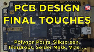
Great video! Really enjoyed learning about Silkscreen & Solder Mask. It was clear and informative. Looking forward to more content like this. Keep up the good work! Phil! Thank you so much for your effort! 👍
Thanks Phil, very helpful for this newbie here, as I've only done a handful of small boards. A few other tricks I have used: - When using inversed text (text as void within solid block), increase minimum stroke width to account for silkscreen bleed. - If you can't have a gap between two designators on one line, a slight vertical misalignment makes it obvious they are two different designators. - Reserve low numbers (i.e. L1..L9, C1-C99) for areas with high component density (i.e. RF matching networks, switching supplies). Question: if you must use a transfer via as a test point, could it be made more durable by adding solder to it?
I recently found your channel when I searched for videos around the PCM2900 usb audio chips and I have to say your videos are brilliant. I have already watched hours and hours of them. I am currently looking into enrolling into your Mixed-Signal Hardware design course and was wandering what the interaction level was like. Is it just videos or would I also be able to ask questions in the comments / email?
Nice one! Btw: Is there a part two where you test two different layouts of switching power supplies? For EMI etc. Did I miss this one or is it coming in the future?
I really do need to get better at giving proper care to the silkscreen but I've always found it incredibly boring so I tend to take shortcuts. This is good motivation though!
I happen to like the 'final bits' of PCB design for some reason. Feels quite relaxing to me and I get to add somewhat of a personal touch with the silkscreen etc.
Good stuff and nice to see 'Center Positive' clearly marked with a little graphic ! Am I right in thinking guitarists pedals have a lot of center negative barrels just to be annoying ?.....cheers.
Thanks, Andy! The center negative thing on guitar pedals is pretty annoying, but does have a reason that if unplugged, we can use the third DC jack terminal for a switched 9V battery connection.
I have mini quadcopter and Zynq-based audio analyser boards/projects in the works at the moment. Should hopefully make for some interesting content I believe!
@@PhilsLab I’ve been following the Zync and audio things for a bit. They are interesting. One thing I wish I saw a bit more videos of on CZcams is quality content for higher voltage things. Roughly 500v. Finding good content with that type of voltage is… “a bit niche”. 🤣🤷♂️
Hey Phil. Been wondering about how you make gold-plated outer edge(which is grounded) like seen on the boards in the beginning. What's the benefit of that? I know it's probably for shielding, but you have ground plane anyways?
I simple add a solder mask opening around the perimeter of the board. To me it's particularly useful as GND probing points all around the PCB (plus it looks cool).
@@PhilsLab What is the width of this? Do you add manually via-s around it? What's the spacing of vias in mm? Adding ENIG surface finish kind of also raises PCB cost. One more question. When speaking about debugging, i haven't seen you use soldered testpoints i mean like keystone soldered testpoints. Have you considered them? Although indeed they take up a lot of space, but really nice to have in debugging stage. Do you happen to solder wires often or how do you connect logic analyzer for example?
Width depends - at least 1mm. Vias are added manually. Spacing depends on max. freq. of signal in design. You don't have to use ENIG. Yes, I solder on wires if I have to - occasionally I'll use soldered turrets/lugs as testpoints.
hi Phill , I need your help please I want to enroll your Advanced Digital Hardware Design course, but I don't know what I should know before and in wich level I am to be sure that I am ready to the course , its doesn't mentioned ! THANK YOU
Hi Phil, a random but relevant question. What is best practice for revision control board design and BOM? How does this fit with the altrium/kicad native file version? Nice videos. Thanks
Hi Ivan, That would make a great video, which I'll be sure to make in the (near) future. For revision control I use Altium 365, or Git for other ECAD tools
Thanks that would be brilliant. I have a specific example that is a little too specific maybe for a video but explains complexities: UK PCB assembly house complained about our revision control (admittedly rightly so). They would prefer both the board and the BOM revision controlled when issued to them for quotation so when an order comes in they know if a simple BOM change has occurred (i.e. simple component substitution) or if a board change has happened. In case of a board change they are handling it as a new project so I understand they will be re-creating the SMT manufacturing line configuration files. Also every time we change something they would like a product change notification that will let them know what has changed from the last board revision. Revision control and PCN allows them to effectively quote for the boards and avoid mistakes. Now, this might be a little different from far east manufacturers where my experience with jlcpcb is that every time the gerbers/bom files are uploaded to the portal. To cut a long story short we are thinking to revision control the PCB gerbers with a major version only and the BOM with the major version of the PCB plus the minor BOM revision. So it could look something like PCB rev 2 and BOM rev 2.3 after 4 BOM revisions. All this seems a little complicated and is certainly new to me.
Phil, Why do you prefer tented vias over non-tented vias? Your arguments aren't convincing for me. How do you comment czcams.com/video/-HNexL-oS-w/video.html BTW: Great video as always.
Many reasons to use tented vias over non-tented (there are exceptions of course, and sometimes reasons not to do). E.g. environmental protection, can place vias closer to pads (reduced inductance) with reduced chance of solder wicking, improving assembly yield. etc. etc. Some further reasons listed here: resources.altium.com/p/when-use-tented-vias-your-pcb-layout


I’m getting back into PCB design after a 2 year hiatus, so I’m watching your videos to remember things I used to know. Thanks!
Awesome, glad you're back to designing - thanks for watching! :)
I love "basics" videos. Searching desperate currently: how to debug, howt to test and how to build testers ... :-)
... and for sure: love your videos, incredible high quality of production.
Great ideas, thank you!
Great series! I would like to suggest a "Ground management 101" video.
Thank you, Antonio - that's a great idea!
Would like to see more advanced BOM mangement with Altium.
Will definitely make a video on BoM strategies and tools, thanks for the suggestion!
Great video! Really enjoyed learning about Silkscreen & Solder Mask. It was clear and informative. Looking forward to more content like this. Keep up the good work! Phil! Thank you so much for your effort! 👍
Thank you very much for your kind comment!
i would be interested in learning more about IPC guidelines and the general sections it covers.
Good idea, that's definitely a topic for a future video I'd like to make!
Yesterday I got my pcb ordered. Was looking for this🙃🙃
Awesome, hope everything works with your PCBs! :)
Thanks, Phil, you produce wonderful content for learning PCB design.
Cheers from Brazil
Thank you!
Thanks Phil, very helpful for this newbie here, as I've only done a handful of small boards. A few other tricks I have used:
- When using inversed text (text as void within solid block), increase minimum stroke width to account for silkscreen bleed.
- If you can't have a gap between two designators on one line, a slight vertical misalignment makes it obvious they are two different designators.
- Reserve low numbers (i.e. L1..L9, C1-C99) for areas with high component density (i.e. RF matching networks, switching supplies).
Question: if you must use a transfer via as a test point, could it be made more durable by adding solder to it?
Great additions, thanks!
Again great video. Thank you.
Thank you, glad you like it!
Very comprehensive as usual. Thanks for the educative video
Thank you!
Great video! Would love to see a video on those multi-coloured/artistic silkscreens.
Thanks, will do when they enable that option!
I recently found your channel when I searched for videos around the PCM2900 usb audio chips and I have to say your videos are brilliant. I have already watched hours and hours of them. I am currently looking into enrolling into your Mixed-Signal Hardware design course and was wandering what the interaction level was like. Is it just videos or would I also be able to ask questions in the comments / email?
Thank you very much! There is a course forum and Discord run by the people at Fedevel, where I also answer questions when they come up.
Nice one! Btw: Is there a part two where you test two different layouts of switching power supplies? For EMI etc. Did I miss this one or is it coming in the future?
Great video as usual - I always learn something new.
Thanks, Mark!
I really do need to get better at giving proper care to the silkscreen but I've always found it incredibly boring so I tend to take shortcuts. This is good motivation though!
I happen to like the 'final bits' of PCB design for some reason. Feels quite relaxing to me and I get to add somewhat of a personal touch with the silkscreen etc.
Good stuff and nice to see 'Center Positive' clearly marked with a little graphic ! Am I right in thinking guitarists pedals have a lot of center negative barrels just to be annoying ?.....cheers.
Thanks, Andy! The center negative thing on guitar pedals is pretty annoying, but does have a reason that if unplugged, we can use the third DC jack terminal for a switched 9V battery connection.
:)@@PhilsLab
Your videos are just top tier
Thank you very much!
Won't you make a video about pi filter with ferrite bead and selecting caps can be driven?
Yes, that's coming - just getting some test boards made that we'll be using together with a Bode100.
Love your videos. Anxiously awaiting the latest headphone amp video. 😎
Thanks! New headphone amp isn't in progress at the moment I'm afraid :(
@@PhilsLab that’s too bad. Hope a different yearly project will come to the fore?
I have mini quadcopter and Zynq-based audio analyser boards/projects in the works at the moment. Should hopefully make for some interesting content I believe!
@@PhilsLab I’ve been following the Zync and audio things for a bit. They are interesting. One thing I wish I saw a bit more videos of on CZcams is quality content for higher voltage things. Roughly 500v. Finding good content with that type of voltage is… “a bit niche”. 🤣🤷♂️
Hey Phil. Been wondering about how you make gold-plated outer edge(which is grounded) like seen on the boards in the beginning. What's the benefit of that? I know it's probably for shielding, but you have ground plane anyways?
In KiCAD it's made with a filled zone on F. B. Mask layers, plus selecting ENIG Surface Finish with your manufacturer.
I simple add a solder mask opening around the perimeter of the board. To me it's particularly useful as GND probing points all around the PCB (plus it looks cool).
@@PhilsLab Additionally such thing significantly reduces EMI level in some cases
@@PhilsLab What is the width of this? Do you add manually via-s around it? What's the spacing of vias in mm? Adding ENIG surface finish kind of also raises PCB cost. One more question. When speaking about debugging, i haven't seen you use soldered testpoints i mean like keystone soldered testpoints. Have you considered them? Although indeed they take up a lot of space, but really nice to have in debugging stage. Do you happen to solder wires often or how do you connect logic analyzer for example?
Width depends - at least 1mm. Vias are added manually. Spacing depends on max. freq. of signal in design. You don't have to use ENIG.
Yes, I solder on wires if I have to - occasionally I'll use soldered turrets/lugs as testpoints.
hi Phill , I need your help please
I want to enroll your Advanced Digital Hardware Design course, but I don't know what I should know before and in wich level I am to be sure that I am ready to the course , its doesn't mentioned !
THANK YOU
Phil, I’m gonna keep asking: what do you use to create your slides? Beamer? Power point?
I use PowerPoint (one of the standard templates) and draw.io for my figures.
Hi Phil, a random but relevant question. What is best practice for revision control board design and BOM? How does this fit with the altrium/kicad native file version? Nice videos. Thanks
Hi Ivan, That would make a great video, which I'll be sure to make in the (near) future. For revision control I use Altium 365, or Git for other ECAD tools
Thanks that would be brilliant. I have a specific example that is a little too specific maybe for a video but explains complexities: UK PCB assembly house complained about our revision control (admittedly rightly so). They would prefer both the board and the BOM revision controlled when issued to them for quotation so when an order comes in they know if a simple BOM change has occurred (i.e. simple component substitution) or if a board change has happened. In case of a board change they are handling it as a new project so I understand they will be re-creating the SMT manufacturing line configuration files. Also every time we change something they would like a product change notification that will let them know what has changed from the last board revision. Revision control and PCN allows them to effectively quote for the boards and avoid mistakes. Now, this might be a little different from far east manufacturers where my experience with jlcpcb is that every time the gerbers/bom files are uploaded to the portal.
To cut a long story short we are thinking to revision control the PCB gerbers with a major version only and the BOM with the major version of the PCB plus the minor BOM revision. So it could look something like PCB rev 2 and BOM rev 2.3 after 4 BOM revisions. All this seems a little complicated and is certainly new to me.
Hi, many thanks
Thanks for watching!
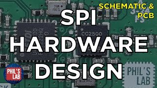
What connector is being used for swd?
Tag-Connect TC2030
please Dear software link
👍🙏❤️
First
Phil, Why do you prefer tented vias over non-tented vias? Your arguments aren't convincing for me. How do you comment czcams.com/video/-HNexL-oS-w/video.html
BTW: Great video as always.
Many reasons to use tented vias over non-tented (there are exceptions of course, and sometimes reasons not to do). E.g. environmental protection, can place vias closer to pads (reduced inductance) with reduced chance of solder wicking, improving assembly yield. etc. etc. Some further reasons listed here: resources.altium.com/p/when-use-tented-vias-your-pcb-layout