Introduction to EBL

Vložit
- čas přidán 22. 01. 2020
- Nanotechnology: A Maker's Course
EBL Basics
Link to the full Coursera course: www.coursera.org/learn/nanote...
************************************************************************
The Shared Materials Instrumentation Facility (SMIF) is the Pratt School of Engineering’s core facility that enables materials, devices, and integrated systems research at Duke University in a variety of fields that include nanotechnology, biomaterials and biomedical engineering, information sciences, optoelectronics, sensor technology, and renewable energy. SMIF is housed in the Fitzpatrick Center for Interdisciplinary Engineering, Medicine and Applied Sciences (FCIEMAS). The facility consists of 7,000 square feet of clean room fabrication space, and nearly 3,000 square feet of specialized laboratory space for characterization and imaging equipment. SMIF is part of the Research Triangle Nanotechnology Network (RTNN) in partnership with similar facilities at North Carolina State University and the University of North Carolina at Chapel Hill. The RTNN is one of 16 organizations nationwide that comprise the National Science Foundation sponsored National Nanotechnology Coordinated Infrastructure (NNCI) program.
SMIF is open to all trained students, staff, faculty, and researchers and is used for both research and educational purposes. SMIF has nearly 700 users, of which 2/3 come from Duke University and 1/3 come from external academic institutions or industry. SMIF staff trains students and researchers to use the lab equipment and instruments themselves, and provides guidance and support in developing processes and methodologies that utilize these capabilities. Alternatively, SMIF staff can run samples for researchers as a service. SMIF also coordinates various educational and outreach activities. - Věda a technologie


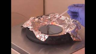


The resist can be positive or negative. Depending on whether it's a positive or negative resist, the exposed resist can be removed or retained respectively, after the development.
Graduate student here, thank you so much for this series. I'll definitely be recommending this in the future!
same xD
Thank you for very good explanation. Your speaking is clear and catchable. It’s easy to understand.
Thank you for this series You helped me a lot in my work
brilliant video, thanks
thank you so much for a such good demonstration
Very informative, thanks.
Hi it is very useful for thanks alot for your great Videos. olease create more such these videos in cleanroom.
Best regards
Nazli
You said: "In development, only the parts of the resist that have been exposed by EBL, will be removed. But this is only true if the resist is a positive resist. If you use a negative resist, all the exposed parts are going to be hardened , and after the development, only the unexposed areas get removed.
Very useful, Thanks.
Thank you, very helpful
very informative video.....
thank you for sharing
Thanku so much 😊😊
Спасибо)
thank you very much for the video. Could you please tell me what are the reasons of the apparance of the stitching lines und why some lithography machine cause this problem and other dont cause this problem?? thank you!
which resist have you used and what was it's thickness after 5000rpm for 40seconds?
How does the acetone reach the EBL resist under the deposited metal layer?
How can I design the lens and beam deflector, what are some books that can be recommended?
its just a crt display, can be directly ripped out of the existing hardware, or 3d printer style printer head moving by small straight on-off electron jet source, you dont even have to use electrons, you can use direct embedding particles, direct printing, picoelectronics and picoelectromechanic systems
Do you know the resolution of the magnitude of the magnetic field used to deflect the electron beam
I don’t know the actual magnitude of the magnetic field generated by the deflection coils. However, regarding beam position resolution: beam positioning is controlled with an 18-bit digital-to-analog controller. The maximum number of discrete positions (horizontally or vertically) is 240,000. The smallest exposure area of the system is 75 micrometers (vertically and horizontally). Thus, the spatial resolution is 75um / 240,000; that is approximately 0.3nm! Just for reference, a human red blood cell is approximately 8,000 nm in diameter… and a human hair is approximately 50,000 - 80,000 nm thick.
EBL just work like the old Cathode Ray Tube TV screen. I am not surprised if China is working on the LED-like beam flat panel Lithography machine now! It should be just a efficient as the Photolithography machine but cheaper!
examples of metals used in lift off??
Chromium, titanium, aluminum, gold, silver, nickel and more
So it's a like an old vacuum tube TV