
- 43
- 111 138
Sentineo Embedded Electronics
Belgium
Registrace 22. 06. 2022
Tips on embedded electronic design for electronic engineers, hobbyists and product designers.
How To Import An Image On Your PCB Silkscreen with Altium
In this quick video, I will show you how to use an exstining image and import it as silkscreen on your PCB. This was a game-changer for me after using a convoluted way with scripts for a long time :-)
Hope this can be of value to you!
If you want more hints, tips and tricks, feel free to join my free community: community.sentineo.com
Hope this can be of value to you!
If you want more hints, tips and tricks, feel free to join my free community: community.sentineo.com
zhlédnutí: 174
Video


USB-C Power Delivery Explained
zhlédnutí 244Před 2 měsíci
How does USB-C power delivery work and what are the different options? In this video I will try to explain this in a way so that you are never confused any more. I will end the video with an actual implementation of a USB-C PD system. If you want more tips & tricks, feel free to join the community here: community.sentineo.com
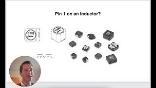
Why Does An Inductor Have A Pin 1?
zhlédnutí 2,2KPřed 2 měsíci
In this video, I will show you why exactly an inductor has a pin 1. This might be an important thing to watch out for in your next SMPS design. Here is a link to the video where I made the power converter design: czcams.com/video/tixEIiC8vjc/video.html If you want more tips & tricks, feel free to join my free community: community.sentineo.com

How To Do PCB Silkscreen Preparation
zhlédnutí 414Před 2 měsíci
In this video I will show you a quick trick how to do PCB silkscreen preparation in Altium Designer. It is a quick and simple method that will save you a lot of time. If you want more tips & tricks like these, feel free to join my free community: community.sentineo.com

3 Easy Ways To Create a PCB Board Shape in Altium
zhlédnutí 1,3KPřed 4 měsíci
In this video I will show you 3 quick ways to create a custom PCB board shape in Altium Designer. If you want more hints, tips and tricks like this, feel free to join my free community at: community.sentineo.com Here is a link to the in-detail video on importing a DXF: czcams.com/video/z5BaFDUAuQI/video.html

Easy Altium Guide To Perfect Impedance Profiles (eg. USB, 50Ω, ...)
zhlédnutí 355Před 4 měsíci
Unlock the secrets of creating perfect impedance profiles in Altium Designer with our easy-to-follow guide! Working on USB, 50Ω, or any other impedance-specific project? This tutorial has got you covered. In this concise step-by-step video, I'll walk you through the process of designing both single and differential tracks, ensuring your PCB designs are optimized and correct. 🔗 Join My Free Comm...

How To Calculate PCB Trace Width for a Power Converter Design
zhlédnutí 1,1KPřed 5 měsíci
In this video, I show you how to calculate the PCB trace width for a power converter PCB layout. Hope this can be valuable to you! For more tips and tricks, feel free to join my free community at: community.sentineo.com Here is a link to the Saturn PCB Toolkit being used in the video: saturnpcb.com/saturn-pcb-toolkit/

How To Solder an SMD Component on a PCB?
zhlédnutí 308Před 5 měsíci
In this quick video, I will show you how to solder an SMD component on a PCB. If you have never done this, check this out first to gain speed. I hope this can be of value to you! If you want more tips & tricks, join my free community here: community.sentineo.com

How To Add a 3D Model For a PCB component Footprint In Altium
zhlédnutí 929Před 5 měsíci
In this quick video, I will show you how to place a 3D STEP body for a PCB component footprint in Altium Designer. Hope this can be valuable for you! If you want more tips on PCB design, feel free to join my free community at: community.sentineo.com For more extended information on component placement, check out a longer video that I made some time ago: czcams.com/video/_sFIKRG66vE/video.html
Super Efficient PCB Component Placement in Altium Designer
zhlédnutí 2KPřed 5 měsíci
In this video I will show you a super efficient way to do component placement on a PCB with Altium Designer. Hope this can be helpful! If you want more tips on PCB design, feel free to join my free community at: community.sentineo.com
How To Do High-Speed Length Tuning in Altium Designer
zhlédnutí 837Před 6 měsíci
In this video, I explain why you need to do length tuning and how you can do that in Altium Designer. If you have any questions, feel free to put them in the comments below in my free online community: community.sentineo.com Hope this video can help you!
How To Design a Rigid Flex PCB in Altium Designer
zhlédnutí 6KPřed 8 měsíci
In this video, I will show you how to design a rigid-flex PCB with Altium Designer. Hope this video can be helpful for you! Feel free to also join the free community for more in-depth tutorials: community.sentineo.com
5 Tips for Perfect PCB Design
zhlédnutí 1KPřed 8 měsíci
In this video I will show you 5 tips to improve your PCB designs massively. If you have any questions, feel free to drop them in the comments below or via our free community: community.sentineo.com Hope this video can be of value to you!
How To Create a Component Library From An Existing Project
zhlédnutí 793Před 9 měsíci
How To Create a Component Library From An Existing Project
How To Run Altium Designer on a Mac M1 or M2 ?
zhlédnutí 6KPřed 11 měsíci
How To Run Altium Designer on a Mac M1 or M2 ?
High Speed PCB Design: How-To? Mastering The Basics For Success
zhlédnutí 4,2KPřed rokem
High Speed PCB Design: How-To? Mastering The Basics For Success
How To Do First Time Right Electronic Design ?
zhlédnutí 261Před rokem
How To Do First Time Right Electronic Design ?
3 Basic Tricks For EMC Compliant PCB Layout
zhlédnutí 8KPřed rokem
3 Basic Tricks For EMC Compliant PCB Layout
How To Check A PCB Layout Before Production?
zhlédnutí 1,2KPřed rokem
How To Check A PCB Layout Before Production?
Altium Designer RF Impedance Matching (e.g. 50Ω, USB, ...)
zhlédnutí 22KPřed rokem
Altium Designer RF Impedance Matching (e.g. 50Ω, USB, ...)
Quick Trick: How To Know Your PCB Will Fail Before Even Assembling It
zhlédnutí 121Před rokem
Quick Trick: How To Know Your PCB Will Fail Before Even Assembling It
The minimal lab equipment for Embedded Hardware Design
zhlédnutí 844Před rokem
The minimal lab equipment for Embedded Hardware Design
Easy BGA eMMC PCB Layout With One Simple Trick
zhlédnutí 2,6KPřed rokem
Easy BGA eMMC PCB Layout With One Simple Trick
Thermal considerations on a PCB Design in Altium Designer
zhlédnutí 979Před rokem
Thermal considerations on a PCB Design in Altium Designer
Why And How To Place Fiducials On A PCB
zhlédnutí 3,7KPřed rokem
Why And How To Place Fiducials On A PCB
Sometimes these NC (No Connect) pins are provided for IC manufacturers to use in factory testing. They may have pull-up and pull-down resistors inside. To use the NC pins, it may be necessary to confirm with the IC manufacturer whether they can be used, otherwise, it may affect signal stability. Additionally, the trace width may vary due to the shape of the PAD, causing the trace width is not smooth.
Very useful. Straight to the point. Thank you.
How is the 3D performance and how well does it handle with complex designs on multiple 4k monitors? I rushed and bought the last gen Intel macbook pro in September 2021 to avoid issues with M series and Altium (as was reported back then by some people). This is my 3rd Intel macbook pro. In a couple of years, would like to upgrade to M series if all the SW issues for EE have been resolved, but looks promising already!
I must confess, never did occur to me to make use of the NC balls. I was thinking of simply pulling some balls from the footprint and simply route underneath them. This seems better, though. As long as you're not unlucky and some NC pins are actually used (as test points, for example) by the manufacturer.
Thanks for your comment, appreciate it.
@@sentineo Thanks for sharing, man. I did check out my favorite mmc's datasheet. Turns out you are correct (ofc you'd be, since you already tried it) - there are NC pins, RFU pins and VSF (vendor special function) pins. All of which are unconnected electrically. I do have one question, if you'd be so kind (since you clearly have more experience than I do). How utterly devastating would you say it would be if I were to place the caps for VDD_CORE (the middle balls) on the same side as the MMC. I'd really like to keep the parts on one side only of my PCB.
Thanks for the video. As far as i know, impedance depends on the signal's frequency. I've read that Altium assumes a frequency of 1GHz for its calculations, but my signal is 1590MHz. Where do i tell Altium this?
Quick and sharp. Thx
Awesome, thank you!
Thanks for making this video! one tip: If you are annoyed by the 'Heads-Up Display' following the mouse cursor, you can move it to the corner and hit Shift-G (Shift-G to move it, Shift-G again to dock it, Shift-H to hide it)
Thanks!
Thanks for making these videos! I'm just commenting to add that after dragging your mouse to select the components, you can type 'TOL' on the PCB side to group by rectangle (shortcut). Even better, if you select components on the SCH one at a time in the order you want to place them (by holding down the SHIFT key), you can type 'TOC' on the PCB side, and they will snap to your mouse cursor one at a time for placement, letting you use your spacebar to rotate before you set it down.
Awesome, thanks for this!
How can you show it even when you are in normal editing mode of the schematic?
Hi, you need to click the tab under the schematic, in this case "03_Peripherals". If you click the tab "editor" you'll see no red crosses, if you select the tab with the schematic name you"ll see your exact variant.
Great Video, is there a way to exclude the logo from the sile2silk constraints?
Hi, you could make it a separate union and then apply a dedicated rule in Altium to it.
thanks for the tip
you're welcome!
Thats great Thank you sir
You're welcome!
Sir, is it possible to design FLEX PCB on Altium 17.4??
I have no clue about that, sorry.
Thank you so much! You have saved me hours.
You're welcome, appreciate your kind words very much! That's what this channel is about, saving you the hassle of trying to find out the same things 🙂
Thanks a lot, never even thought about this. Now I will always be aware of it 🙂 czcams.com/video/k9ANAzAe6fA/video.html
Great video! One question: are you assuming the conductor width and via diameter and checking which conductor current values end up being output or is there some calculation behind your choice of width please? Thanks :)
Indeed, it is an iterative process where I manually alter these values in the calculator tool to see how closely they match up to my needs. When I have found a value that works, I will typically include some extra margin (20%). Hope this answers your question?
Hello, first of all, thank you very much for these great contributions to your channel. My question is about what is the distance between vias for shielding the RF line to reduce crosstalk? How is the distance between tracks calculated to shield a 4G LTE/NB-IoT RF line and what diameter and hole should the vias be? thank you very much, greetings!
Thanks for the kind words, much appreciated! Ideally, it's best not to place the shielding too close. Best to also respect the 3x linewidth rule here for spacing to via fences. In terms of diameters, I would go with your standard (minimal) via size. Respecting the distance however is important: rule of thumb for stitching via spacing (when it comes to RF shielding), is to have a distance of at least 1/10th of the wavelength of your signal. So for e.g. a signal of 1.9GHz, the wavelength is ~158mm - a distance of 15.8mm would be enough to effectively contain a pure sine wave.
Nice vid Would be helpful if you included the keyboard presses you do as you zip across altium and it would be great to learn the shortcuts.
Thanks for your comment. Good suggestion, will keep this in mind for future videos!
Can it supply bidirectional power ? I mean if I want to design USB hub and want to charge upstream device and transfer data, can I use it?
This controller will only work for power delivery. If you want a combination with data exchange in DFP/UFP/DRP mode typically you would combine it with a device like this: www.ti.com/lit/ds/symlink/hd3ss3220.pdf
@@sentineo Actually my question was wrong. I need PD IC which has power role swap to combine it with HD3SS3220.
Is there any type of filtering required for EMI/EMC. I have designed a microcontroller board , it has many other IC's. its working perfectly. but little problem of EMI/EMC. Is it possible for you to review my PCB ?
Hi, best to post this question in the community: community.sentineo.com
Thank you for sharing.
You're welcome!
Love it to the point absolutely amazing ! You got one more subscriber.
Thanks, appreciate the nice words!
Very nicely put together and explained, thank you!
Great to hear! Thanks for the kind words.
Excellent! This question came up in the shop a couple of days ago. I’ll share the information and enlighten the crew. Thank you!
You're welcome, great to hear!
Nice that you show the more advance functions
Awesome videos, your channel is underrated.
Thanks for your warm comment! Appreciate it very much!
Thanks
You're welcome!
Thanks for sharing!
You're welcome!
nice video!
Thank you!
good video
Thanks!
Great explanation, you deserve a sub!. I never ever realize the meaning behind the marked pin let alone I Don't even notice it 😂
Thanks, appreciate your comment! I only realized it after being in electronics for a long time as well 😂 So I thought, might as well share 😄
Thanks for your video. It makes sense if the inductor is asymetrical, but surely if you wind up the former from bottom to top and then down again to the bottom you get a fully symetrical inductor where both pins are equivalent. However real coils always have a pin 1 marked - so how do you know ?
You could of course ask the manufacturer of the coil. If they don't know whats inside theyr own inductors, they don't deserve to be in business anymore. Another way might be to take one apart, and look for yourself how its built. Generally tho, just follow the guidelines and use pin 1 on the switching node side will probably get you in the right direction pretty much almost all the time.
Very Nice ,Thank You.
You're welcome, glad you liked it!
thank you for the clear explanation
You're welcome!
Thank you! I will update my PCB asap!
You're welcome! And the great news is, it's just a small tweak to make on your PCB 😄
Interesting
Glad to hear you like it!
I really appreciated your detailed explanation of preparing the PCB Silkscreen. The video was excellent. Is there any possibility of accomplishing the same task using a plugin in KiCAD, instead of updating each footprint individually?
Thanks for you nice comment! I personally don't know if there's a similar option in KiCAD, but maybe someone can chime in here? Or feel free to ask the question in the community (see link in the description). Probably someone in there that can help.
Thanks for the tutorial. I did that and it work, I see the 3D model in 3D view of the footprint, but now, I tried so many steps, saving in another file etc, but I cannot use that component/footprint in my other projects, could you please show a complete workflow of doing so ? It just a few seconds more after when this video ended I suppose.
Please make sure that it is in a component library that is also included in your project. If your component lib is not included, you won't be able to use a component.
Thank You Very Much Sir.
You're welcome!
Thanks for the video, I'm working on a rigid/flex design and need some help: I need to put some resistors on the flex layer, I've been able to do it, but the silkscreen doesn't transfer to the Flex Overlay, is this possible to do? Do the components need to be made specifically for the internal layer? Also, when I add the flex layers, the Top and Bottom Overlays are no longer visible in the View Configurations Panel, they get replaced with the Flex Top and Bottom Overlays, is this correct? Thanks for your help.
For the second part of your question: indeed it is correct that this has become Flex Top and Bottom Overlays. For the first part, I don't fully understand your quesion?
Thank you so much
You're welcome, glad you liked it!
can you please make another video on flexible routing traces..
Thanks great stuff, going to check out your full length videos again
Awesome, thank you!
Just did a whole pcb layout, but then with multi select and ordening everything by hand... Thanks for this tip
Very welcome!
One of the very best video s I´ve ever seen about these features. Thank you.
Glad that this video was helpful! Appreciate the kind words very much, thank you.
really appreciate your tutorial, very easy to follow
Thanks, glad to hear this!
Great video as always. I would recommend you to start series video on altium designer. Thanks in advance
Thank you! Your video has answered many questions I had about the rigid-flex design!
Thanks, great to hear that. Much appreciated!
This is so good!!
Thanks!
Thanks for the nice Video
Thank you, appreciate the kind words!